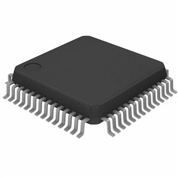
- 封装:56-TFSOP(0.240",6.10mm 宽)
- RoHS:无铅 / 符合限制有害物质指令(RoHS)规范要求
- 包装方式:Digi-Reel®
- 参考价格:$1.512-$3.02
更新日期:2024-04-01 00:04:00
产品简介:具有三态输出的 3.3V ABT 18 位通用总线驱动器
查看详情- 封装:56-TFSOP(0.240",6.10mm 宽)
- RoHS:无铅 / 符合限制有害物质指令(RoHS)规范要求
- 包装方式:Digi-Reel®
- 参考价格:$1.512-$3.02
SN74LVTH16835DGGR 供应商
- 公司
- 型号
- 品牌
- 封装/批号
- 数量
- 地区
- 日期
- 说明
- 询价
-
TI
-
原厂原装
22+ -
3288
-
上海市
-
-
-
一级代理原装
-
TI
-
-
2019+ -
5800
-
上海市
-
-
-
全新原装现货
-
TI(德州仪器)
-
TSSOP-56
2022+ -
12000
-
上海市
-
-
-
原装可开发票
SN74LVTH16835DGGR 中文资料属性参数
- 标准包装:1
- 类别:集成电路 (IC)
- 家庭:逻辑 - 通用总线函数
- 系列:74LVTH
- 逻辑类型:通用总线驱动器
- 输入数:-
- 电路数:18 位
- 输出电流高,低:32mA,64mA
- 电源电压:2.7 V ~ 3.6 V
- 工作温度:-40°C ~ 85°C
- 安装类型:表面贴装
- 封装/外壳:56-TFSOP(0.240",6.10mm 宽)
- 供应商设备封装:56-TSSOP
- 包装:®
- 其它名称:296-8694-6
产品特性
- Members of the Texas Instruments WidebusTM Family
- State-of-the-Art Advanced BiCMOS Technology (ABT) Design for 3.3-V Operation and Low Static-Power Dissipation
- Support Mixed-Mode Signal Operation (5-V Input and Output Voltages With 3.3-V VCC)
- Support Unregulated Battery Operation Down to 2.7 V
- Typical VOLP (Output Ground Bounce) < 0.8 V at VCC = 3.3 V, TA = 25°C
- Ioff and Power-Up 3-State Support Hot Insertion
- Bus Hold on Data Inputs Eliminates the Need for External Pullup/Pulldown Resistors
- Distributed VCC and GND Pin Configuration Minimizes High-Speed Switching Noise
- Flow-Through Architecture Optimizes PCB Layout
- Latch-Up Performance Exceeds 500 mA Per JESD 17
- ESD Protection Exceeds 2000 V Per MIL-STD-883, Method 3015; Exceeds 200 V Using Machine Model (C = 200 pF, R = 0)
- Package Options Include Plastic Shrink Small-Outline (DL) and Thin Shrink Small-Outline (DGG) Packages and 380-mil Fine-Pitch Ceramic Flat (WD) Package Using 25-mil Center-to-Center Spacings Widebus is a trademark of Texas Instruments Incorporated.
产品概述
The 'LVTH16835 devices are 18-bit universal bus drivers designed for low-voltage (3.3-V) VCC operation, but with the capability to provide a TTL interface to a 5-V system environment.
Data flow from A to Y is controlled by the output-enable (OE\) input. These devices operate in the transparent mode when the latch-enable (LE) input is high. The A data is latched if the clock (CLK) input is held at a high or low logic level. If LE is low, the A data is stored in the latch/flip-flop on the low-to-high transition of the clock. When OE\ is high, the outputs are in the high-impedance state.
Active bus-hold circuitry is provided to hold unused or floating data inputs at a valid logic level.
When VCC is between 0 and 1.5 V, the devices are in the high-impedance state during power up or power down. However, to ensure the high-impedance state above 1.5 V, OE\ should be tied to VCC through a pullup resistor; the minimum value of the resistor is determined by the current-sinking capability of the driver.
These devices are fully specified for hot-insertion applications using Ioff and power-up 3-state. The Ioff circuitry disables the outputs, preventing damaging current backflow through the devices when they are powered down. The power-up 3-state circuitry places the outputs in the high-impedance state during power up and power down, which prevents driver conflict.
The SN54LVTH16835 is characterized for operation over the full military temperature range of -55°C to 125°C. The SN74LVTH16835 is characterized for operation from -40°C to 85°C.
SN74LVTH16835DGGR 数据手册
| 数据手册 | 说明 | 数量 | 操作 |
|---|---|---|---|
 SN74LVTH16835DGGR SN74LVTH16835DGGR
|
Universal Bus Driver 18-Bit 56-TSSOP |
15页,1003K | 查看 |
SN74LVTH16835DGGR 相关产品
- 74ALVCH16501DGGRG4
- 74LVTH16501DGGRE4
- CD74HC299E
- CD74HC299M96
- CD74HCT299E
- CD74HCT299M96
- CVMEH22501AIDGGREP
- CVMEH22501AIDGVREP
- GTLP18T612MTDX
- SN74ABT162500DL
- SN74ABT162601DGGR
- SN74ABT162601DLR
- SN74ABT16500BDGGR
- SN74ABT16500BDL
- SN74ABT16500BDLR
- SN74ABT16501DGGR
- SN74ABT16501DL
- SN74ABT16501DLR
- SN74ABT16601DGGR
- SN74ABT16601DL
- SN74ABT16601DLR
- SN74ABTH182502APM
- SN74ABTH182504APM
- SN74ABTH18502APM
- SN74ABTH18502APMR
- SN74ABTH18504APM
- SN74ABTH32316PN
- SN74ABTH32318PN
- SN74ALVC162334DGGR
- SN74ALVC162334DGVR

 搜索
搜索
 发布采购
发布采购
