 搜索
搜索
 发布采购
发布采购
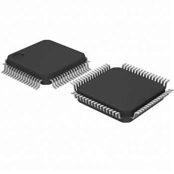
- 封装:64-LQFP
- RoHS:无铅 / 符合限制有害物质指令(RoHS)规范要求
- 包装方式:Digi-Reel®
- 参考价格:$13.857-$21.11
更新日期:2024-04-01 00:04:00
产品简介:具有 18 位通用总线收发器的扫描测试设备
查看详情- 封装:64-LQFP
- RoHS:无铅 / 符合限制有害物质指令(RoHS)规范要求
- 包装方式:Digi-Reel®
- 参考价格:$13.857-$21.11
SN74ABTH18502APMR 供应商
- 公司
- 型号
- 品牌
- 封装/批号
- 数量
- 地区
- 日期
- 说明
- 询价
-
TI
-
原厂原装
22+ -
3288
-
上海市
-
-
-
一级代理原装
-
TI(德州仪器)
-
LQFP-64
2022+ -
12000
-
上海市
-
-
-
原装可开发票
SN74ABTH18502APMR 中文资料属性参数
- 标准包装:1
- 类别:集成电路 (IC)
- 家庭:逻辑 - 通用总线函数
- 系列:74ABTH
- 逻辑类型:扫描测试通用总线收发器
- 输入数:-
- 电路数:18 位
- 输出电流高,低:32mA,64mA
- 电源电压:4.5 V ~ 5.5 V
- 工作温度:-40°C ~ 85°C
- 安装类型:表面贴装
- 封装/外壳:64-LQFP
- 供应商设备封装:64-LQFP(10x10)
- 包装:®
- 其它名称:296-14683-6
产品特性
- Members of the Texas Instruments SCOPETM Family of Testability Products
- Members of the Texas Instruments WidebusTM Family
- Compatible With the IEEE Standard 1149.1-1990 (JTAG) Test Access Port and Boundary-Scan Architecture
- UBTTM (Universal Bus Transceiver) Combines D-Type Latches and D-Type Flip-Flops for Operation in Transparent, Latched, or Clocked Mode
- Bus Hold on Data Inputs Eliminates the Need for External Pullup Resistors
- B-Port Outputs of 'ABTH182502A Devices Have Equivalent 25- Series Resistors, So No External Resistors Are Required
- State-of-the-Art EPIC-IIBTM BiCMOS Design
- One Boundary-Scan Cell Per I/O Architecture Improves Scan Efficiency
- SCOPE Instruction Set IEEE Standard 1149.1-1990 Required Instructions and Optional CLAMP and HIGHZ Parallel-Signature Analysis at Inputs Pseudo-Random Pattern Generation From Outputs Sample Inputs/Toggle Outputs Binary Count From Outputs Device Identification Even-Parity Opcodes
- IEEE Standard 1149.1-1990 Required Instructions and Optional CLAMP and HIGHZ
- Parallel-Signature Analysis at Inputs
- Pseudo-Random Pattern Generation From Outputs
- Sample Inputs/Toggle Outputs
- Binary Count From Outputs
- Device Identification
- Even-Parity Opcodes
- Packaged in 64-Pin Plastic Thin Quad Flat (PM) Packages Using 0.5-mm Center-to-Center Spacings and 68-Pin Ceramic Quad Flat (HV) Packages Using 25-mil Center-to-Center Spacings SCOPE, Widebus, UBT, and EPIC-IIB are trademarks of Texas Instruments Incorporated.
产品概述
The 'ABTH18502A and 'ABTH182502A scan test devices with 18-bit
universal bus transceivers are members of the Texas Instruments SCOPE
testability integrated-circuit family. This family of devices
supports IEEE Standard 1149.1-1990 boundary scan to facilitate
testing of complex circuit-board assemblies. Scan access to the test
circuitry is accomplished via the 4-wire test access port (TAP)
interface.In the normal mode, these devices are 18-bit universal bus
transceivers that combine D-type latches and D-type flip-flops to
allow data flow in transparent, latched, or clocked modes. They can
be used either as two 9-bit transceivers or one 18-bit transceiver.
The test circuitry can be activated by the TAP to take snapshot
samples of the data appearing at the device pins or to perform a self
test on the boundary-test cells. Activating the TAP in the normal
mode does not affect the functional operation of the SCOPE universal
bus transceivers.Data flow in each direction is controlled by output-enable ( and ), latch-enable (LEAB and LEBA),
and clock (CLKAB and CLKBA) inputs. For A-to-B data flow, the device
operates in the transparent mode when LEAB is high. When LEAB is low,
the A-bus data is latched while CLKAB is held at a static low or high
logic level. Otherwise, if LEAB is low, A-bus data is stored on a
low-to-high transition of CLKAB. When is low, the B outputs are active.
When is high, the B
outputs are in the high-impedance state. B-to-A data flow is similar
to A-to-B data flow but uses the , LEBA, and CLKBA inputs.In the test mode, the normal operation of the SCOPE universal bus
transceivers is inhibited and the test circuitry is enabled to
observe and control the I/O boundary of the device. When enabled, the
test circuitry performs boundary-scan test operations according to
the protocol described in IEEE Standard 1149.1-1990. Four dedicated test pins observe and control the operation of the
test circuitry: test data input (TDI), test data output (TDO), test
mode select (TMS), and test clock (TCK). Additionally, the test
circuitry performs other testing functions such as parallel-signature
analysis (PSA) on data inputs and pseudo-random pattern generation
(PRPG) from data outputs. All testing and scan operations are
synchronized to the TAP interface.Improved scan efficiency is accomplished through the adoption of a
one boundary-scan cell (BSC) per I/O pin architecture. This
architecture is implemented in such a way as to capture the most
pertinent test data. A PSA/COUNT instruction also is included to ease
the testing of memories and other circuits where a binary count
addressing scheme is useful.Active bus-hold circuitry holds unused or floating data inputs at
a valid logic level.The B-port outputs of 'ABTH182502A, which are designed to source
or sink up to 12 mA, include 25- series resistors to reduce overshoot and undershoot.
The SN54ABTH18502A and SN54ABTH182502A are characterized for
operation over the full military temperature range of -55°C to
125°C. The SN74ABTH18502A and SN74ABTH182502A are characterized
for operation from -40°C to 85°C. A-to-B data flow is shown. B-to-A data flow is similar but
uses OEBA\, LEBA, and CLKBA.Output level before the indicated steady-state input
conditions were established
SN74ABTH18502APMR 数据手册
| 数据手册 | 说明 | 数量 | 操作 |
|---|---|---|---|
 SN74ABTH18502APMR SN74ABTH18502APMR
|
Scan Test Universal Bus Transceiver 18-Bit 64-LQFP (10x10) |
43页,965K | 查看 |
SN74ABTH18502APMR 相关产品
- 74ALVCH16501DGGRG4
- 74LVTH16501DGGRE4
- CD74HC299E
- CD74HC299M96
- CD74HCT299E
- CD74HCT299M96
- CVMEH22501AIDGGREP
- CVMEH22501AIDGVREP
- GTLP18T612MTDX
- SN74ABT162500DL
- SN74ABT162601DGGR
- SN74ABT162601DLR
- SN74ABT16500BDGGR
- SN74ABT16500BDL
- SN74ABT16500BDLR
- SN74ABT16501DGGR
- SN74ABT16501DL
- SN74ABT16501DLR
- SN74ABT16601DGGR
- SN74ABT16601DL
- SN74ABT16601DLR
- SN74ABTH182502APM
- SN74ABTH182504APM
- SN74ABTH18502APM
- SN74ABTH18504APM
- SN74ABTH32316PN
- SN74ABTH32318PN
- SN74ALVC162334DGGR
- SN74ALVC162334DGVR
- SN74ALVC162334DLR