 搜索
搜索
 发布采购
发布采购
AOD418
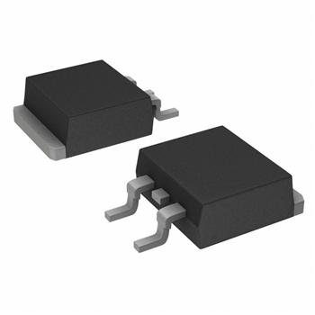
FET - 单- 封装:TO-252-3,DPak(2 引线+接片),SC-63
- RoHS:无铅 / 符合限制有害物质指令(RoHS)规范要求
- 包装方式:带卷 (TR)
- 参考价格:$0.198
更新日期:2024-04-01 00:04:00
AOD418
FET - 单产品简介:MOSFET N-CH 30V 13.5A TO252
- 封装:TO-252-3,DPak(2 引线+接片),SC-63
- RoHS:无铅 / 符合限制有害物质指令(RoHS)规范要求
- 包装方式:带卷 (TR)
- 参考价格:$0.198
AOD418 供应商
- 公司
- 型号
- 品牌
- 封装/批号
- 数量
- 地区
- 日期
- 说明
- 询价
-
AOD418
原装现货 -
韦盛/VSEEI
-
TO-252
24+ -
81284
-
深圳
-
11-22
-
只做大芯片/可代替进口/可订制
-
AO代理
-
TO252
23+ -
15000
-
上海市
-
-
-
中国区代理原装进口特价
-
AOS/ELNAF
-
SOT252
1901+ -
5000
-
上海市
-
-
-
原装现货,精专配套,正品BOM表报价
-
AOS/万代
-
TO-252
21+ -
16500
-
杭州
-
-
-
只做原装现货,大量现货热卖
-
AOS原装新货
-
TO252
22+授权代理 -
15800
-
上海市
-
-
-
旋尔只做进口原装,假一赔十...
-
AOS
-
TO-252
新批号 -
887000
-
上海市
-
-
-
原厂发货进口原装微信同步QQ893727827
-
AOS
-
SOT252
23+ -
5800
-
上海市
-
-
-
进口原装现货,杜绝假货。
-
AOS
-
TO-252
- -
10
-
上海市
-
-
-
经营22年实体店原装,具体年份和数量以实际为准
-
AOS
-
-
21+ -
2500
-
上海市
-
-
-
原装现货,品质为先,请来电垂询!
-
VBSEMI/台湾微碧
-
TO-252
24+ -
1000
-
深圳
-
-
-
只做原装,好价支持
AOD418 中文资料属性参数
- 标准包装:2,500
- 类别:分离式半导体产品
- 家庭:FET - 单
- 系列:-
- FET 型:MOSFET N 通道,金属氧化物
- FET 特点:逻辑电平门
- 漏极至源极电压(Vdss):30V
- 电流 - 连续漏极(Id) @ 25° C:13.5A
- 开态Rds(最大)@ Id, Vgs @ 25° C:7.5 毫欧 @ 20A,10V
- Id 时的 Vgs(th)(最大):2.5V @ 250µA
- 闸电荷(Qg) @ Vgs:24nC @ 10V
- 输入电容 (Ciss) @ Vds:1380pF @ 15V
- 功率 - 最大:2.5W
- 安装类型:表面贴装
- 封装/外壳:TO-252-3,DPak(2 引线+接片),SC-63
- 供应商设备封装:TO-252
- 包装:带卷 (TR)
AOD418 数据手册
| 数据手册 | 说明 | 数量 | 操作 |
|---|---|---|---|
 AOD4186 AOD4186
|
(V GS = 10V) (V GS = 10V) (V GS = 4.5V) Symbol V DS V GS I DM I AR E AR T J , T STG Symbol Typ Max 16.7 25 40 50 R θJC 2.5 3 I D = 35A R DS(ON) < 15m? T C =25°C 2.5 25 T C =100°C 24 70 Pulsed Drain Current C Continuous Drain Current G Junction and Storage Temperature Range -55 to 175 °C Thermal Characteristics Units Maximum Junction-to-Ambient A t ≤ 10s °C/W Parameter R θJA V V ±20 Gate-Source Voltage Drain-Source Voltage 40 AOD4186 Maximum Units Parameter Absolute Maximum Ratings T A =25°C unless otherwise noted The AOD4186 combines advanced trench MOSFET technology with a low resistance package to provide extremely low R DS(ON) . This device is ideal for low voltage inverter applications. R DS(ON) < 19m? V DS (V) =40V Repetitive avalanche energy L=0.1mH C mJ Avalanche Current C 8 Continuous Drain Current 29 10 A A T A =25°C I DSM A T A =70°C I D 35 27 T C =25°C T C =100°C Power Dissipation B P D W Power Dissipation A P DSM W T A =70°C 50 1.6 T A =25°C Maximum J |
6页,458K | 查看 |
|
AOD4186
|
General Description Features (V GS = 10V) (V GS = 10V) (V GS = 4.5V) - RoHS Compliant 100% UIS Tested! - Halogen Free 100% R g Tested! Symbol V DS V GS I DM I AR E AR T J , T STG Symbol Typ Max 16.7 25 40 50 R θJC 2.5 3 I D = 50A R DS(ON) < 15m? T C =25°C 2.5 25 T C =100°C 24 70 Pulsed Drain Current C Continuous Drain Current G Junction and Storage Temperature Range -55 to 175 °C Thermal Characteristics Units Maximum Junction-to-Ambient A t ≤ 10s °C/W Parameter R θJA V V ±20 Gate-Source Voltage Drain-Source Voltage 40 AOD4186 N-Channel Enhancement Mode Field Effect Transistor Maximum Units Parameter Absolute Maximum Ratings T A =25°C unless otherwise noted The AOD4186 combines advanced trench MOSFET technology with a low resistance package to provide extremely low R DS(ON) . This device is ideal for low voltage inverter applications. R DS(ON) < 19m? V DS (V) =40V Repetitive avalanche energy L=0.1mH C mJ Avalanche Current C 8 Continuous Drain Current 29 10 A A T |
6页,154K | 查看 |
|
AOD4186_829
|
(V GS = 10V) (V GS = 10V) (V GS = 4.5V) Symbol V DS V GS I DM I AR E AR T J , T STG Symbol Typ Max 16.7 25 40 50 R θJC 2.5 3 I D = 35A R DS(ON) < 15m? T C =25°C 2.5 25 T C =100°C 24 70 Pulsed Drain Current C Continuous Drain Current G Junction and Storage Temperature Range -55 to 175 °C Thermal Characteristics Units Maximum Junction-to-Ambient A t ≤ 10s °C/W Parameter R θJA V V ±20 Gate-Source Voltage Drain-Source Voltage 40 AOD4186 Maximum Units Parameter Absolute Maximum Ratings T A =25°C unless otherwise noted The AOD4186 combines advanced trench MOSFET technology with a low resistance package to provide extremely low R DS(ON) . This device is ideal for low voltage inverter applications. R DS(ON) < 19m? V DS (V) =40V Repetitive avalanche energy L=0.1mH C mJ Avalanche Current C 8 Continuous Drain Current 29 10 A A T A =25°C I DSM A T A =70°C I D 35 27 T C =25°C T C =100°C Power Dissipation B P D W Power Dissipation A P DSM W T A =70°C 50 1.6 T A =25°C Maximum J |
6页,458K | 查看 |
AOD418 相关产品
- 2N7000
- 2N7000BU
- 2N7000G
- 2N7000RLRAG
- 2N7000RLRMG
- 2N7000TA
- 2N7002
- 2N7002,215
- 2N7002-7-F
- 2N7002A-7
- 2N7002BK,215
- 2N7002BKM,315
- 2N7002BKT,115
- 2N7002BKW,115
- 2N7002E
- 2N7002E,215
- 2N7002E-7-F
- 2N7002E-T1-E3
- 2N7002ET1G
- 2N7002E-T1-GE3
- 2N7002F,215
- 2N7002K
- 2N7002K-7
- 2N7002K-T1-E3
- 2N7002KT1G
- 2N7002K-T1-GE3
- 2N7002K-TP
- 2N7002LT1
- 2N7002LT1G
- 2N7002LT3G