 搜索
搜索
 发布采购
发布采购
更新日期:2024-04-01 00:04:00

产品简介:适用于 GaNFET 和 MOSFET 且具有 5V UVLO 的 5kVrms、4A/6A 单通道隔离式栅极驱动器
查看详情UCC5304DWVR 供应商
- 公司
- 型号
- 品牌
- 封装/批号
- 数量
- 地区
- 日期
- 说明
- 询价
-
TI
-
原厂原装
22+ -
3288
-
上海市
-
-
-
一级代理原装
UCC5304DWVR 中文资料属性参数
- 现有数量:2,231现货10,000Factory
- 价格:1 : ¥19.08000剪切带(CT)1,000 : ¥9.72247卷带(TR)
- 系列:Automotive, AEC-Q100
- 包装:卷带(TR)剪切带(CT)? 得捷定制卷带
- 产品状态:在售
- 技术:容性耦合
- 通道数:1
- 电压 - 隔离:5000Vrms
- 共模瞬变抗扰度(最小值):100V/ns
- 传播延迟 tpLH / tpHL(最大值):40ns,40ns
- 脉宽失真(最大):5.5ns
- 上升/下降时间(典型值):5ns,6ns
- 电流 - 输出高、低:4A,6A
- 电流 - 峰值输出:4A,6A
- 电压 - 正向 (Vf)(典型值):-
- 电流 - DC 正向 (If)(最大值):-
- 电压 -?输出供电:6V ~ 18V
- 工作温度:-40°C ~ 125°C
- 安装类型:表面贴装型
- 封装/外壳:8-SOIC(0.295",7.50mm 宽)
- 供应商器件封装:8-SOIC
- 认证机构:CQC,UL,VDE
产品特性
- Reinforced isolation
- Single channel in DWV Package with 8.5-mm creepage distance
- CMTI greater than 100-V/ns
- 4-A peak source, 6-A peak sink output
- Switching parameters: 40-ns maximum propagation delay 5-ns maximum delay matching 5.5-ns maximum pulse-width distortion 35-µs maximum VDD power-up delay
- 40-ns maximum propagation delay
- 5-ns maximum delay matching
- 5.5-ns maximum pulse-width distortion
- 35-µs maximum VDD power-up delay
- Up to 18-V VDD output drive supply 5-V VDD UVLO
- 5-V VDD UVLO
- Operating temp. range (TA) –40°C to 125°C
- Rejects input pulses shorter than 5-ns
- TTL and CMOS compatible inputs
产品概述
The UCC5304 device is an isolated single-channel gate driver with 4-A peak-source and 6-A
peak-sink current. It is designed to drive power MOSFETs and GaNFETs in PFC, Isolated AC/DC, DC/DC,
and synchronous rectification applications, with fast switching performance and robust ground
bounce protection through greater than 100-V/ns common-mode transient immunity (CMTI).The UCC5304 is available in a 8.5 mm SOIC-8 (DWV) package and can support isolation
voltage up to 5-kVRMS. Compared to an optocoupler, the UCC5304 family has
lower part-to-part skew, lower propagation delay, higher operating temperature, and higher
CMTI.Protection features include: IN pin rejects input transient shorter than 5-ns; both input
and output can withstand –2-V spikes for 200-ns, both supplies have undervoltage lockout (UVLO),
and active pull down protection clamps the output below 2.1-V when unpowered or floated.With these features, this device enables high efficiency, high power density, and
robustness in a wide variety of power applications.
UCC5304DWVR 电路图
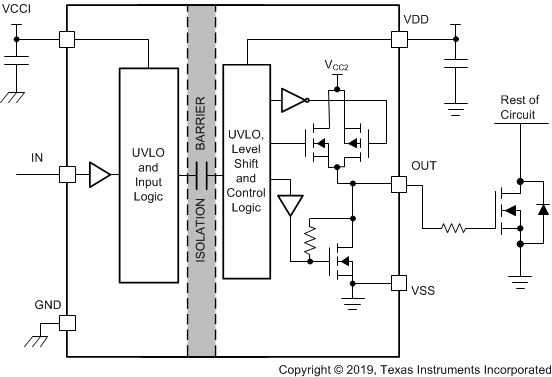
UCC5304DWVR 电路图
UCC5304DWVR 相关产品
- ADUM3220WBRZ
- FOD8316
- FOD8316R2
- ISO5451DW
- ISO5451DWR
- ISO5451QDWQ1
- ISO5451QDWRQ1
- ISO5452DW
- ISO5452DWR
- ISO5452QDWQ1
- ISO5452QDWRQ1
- ISO5851DW
- ISO5851DWR
- ISO5851QDWQ1
- ISO5851QDWRQ1
- ISO5852SDW
- ISO5852SDWR
- ISO5852SMDWREP
- ISO5852SQDWQ1
- ISO5852SQDWRQ1
- SI8261ACC-C-IS
- SI8261BCD-C-IS
- TLP352(TP1,F)
- UCC20225AQNPLRQ1
- UCC20225AQNPLTQ1
- UCC20225NPLR
- UCC20225NPLT
- UCC20225QNPLRQ1
- UCC20225QNPLTQ1
- UCC20520DW