 搜索
搜索
 发布采购
发布采购
更新日期:2024-04-01 00:04:00

产品简介:具有可编程死区时间且采用 DWK 封装的汽车类 3.75kVrms、4A/6A 双通道隔离式栅极驱动器
查看详情UCC21320QDWKQ1 供应商
- 公司
- 型号
- 品牌
- 封装/批号
- 数量
- 地区
- 日期
- 说明
- 询价
-
TI
-
原厂原装
22+ -
3288
-
上海市
-
-
-
一级代理原装
-
TI(德州仪器)
-
SOIC-14
2022+ -
12000
-
上海市
-
-
-
原装可开发票
UCC21320QDWKQ1 中文资料属性参数
- 现有数量:0现货查看交期
- 价格:1 : ¥48.81000管件
- 系列:Automotive, AEC-Q100
- 包装:管件
- 产品状态:在售
- 技术:容性耦合
- 通道数:2
- 电压 - 隔离:3750Vrms
- 共模瞬变抗扰度(最小值):100V/ns
- 传播延迟 tpLH / tpHL(最大值):30ns,30ns
- 脉宽失真(最大):6ns
- 上升/下降时间(典型值):6ns,7ns
- 电流 - 输出高、低:4A,6A
- 电流 - 峰值输出:4A,6A
- 电压 - 正向 (Vf)(典型值):-
- 电流 - DC 正向 (If)(最大值):-
- 电压 -?输出供电:9.2V ~ 25V
- 工作温度:-40°C ~ 125°C
- 安装类型:表面贴装型
- 封装/外壳:14-SOIC(0.295",7.50mm 宽)
- 供应商器件封装:14-SOIC
- 认证机构:CQC,UL,VDE
产品特性
- 4-A peak source, 6-A peak sink output
- 3-V to 18-V input VCCI range to interface with both digital and analog controllers
- Up to 25-V VDD output drive supply
- Switching parameters: 19-ns typical propagation delay 10-ns minimum pulse width 5-ns maximum delay matching 6-ns maximum pulse-width distortion
- 19-ns typical propagation delay
- 10-ns minimum pulse width
- 5-ns maximum delay matching
- 6-ns maximum pulse-width distortion
- Common-mode transient immunity (CMTI) greater than 100 V/ns
- Universal: dual low-side, dual high-side or half-bridge driver
- Programmable overlap and dead time
- Wide Body SOIC-14 (DWK) Package 3.3mm spacing between driver channels
- 3.3mm spacing between driver channels
- Operating temperature range –40 to +125°C
- Surge immunity up to 12.8 kV
- Isolation barrier life >40 years
- TTL and CMOS compatible inputs
- Rejects input pulses and noise transients shorter than 5 ns
- Fast disable for power sequencing
- Qualified for automotive applications
- AEC-Q100 qualified with the following results Device temperature grade 1 Device HBM ESD classification level H2 Device CDM ESD classification level C6
- Device temperature grade 1
- Device HBM ESD classification level H2
- Device CDM ESD classification level C6
产品概述
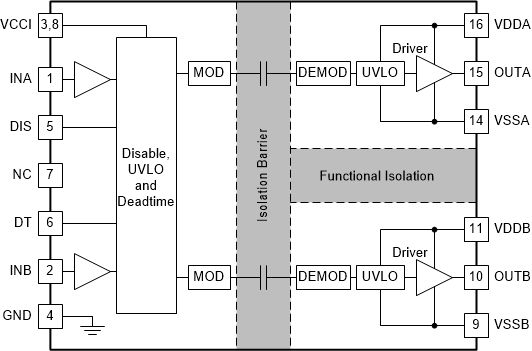
The UCC21320-Q1
is an isolated dual-channel gate
drivers with 4-A source and 6-A sink peak current. It is designed to drive power MOSFETs, IGBTs,
and SiC MOSFETs up to 5-MHz with best-in-class propagation delay and pulse-width distortion.
The input side is isolated from the two output drivers by a
3.75-kVRMS basic isolation barrier, with a minimum of 100-V/ns common-mode
transient immunity (CMTI). Internal functional isolation between the two secondary-side drivers
allows a working voltage of up to 1500 VDC.Every driver can be configured as two low-side drivers, two high-side
drivers, or a half-bridge driver with programmable dead time (DT). A disable pin shuts down both
outputs simultaneously, and allows normal
operation when left open or grounded. As a fail-safe measure, primary-side logic failures force
both outputs low.Each device accepts VDD supply voltages up to 25 V. A wide input VCCI range
from 3 V to 18 V makes the driver suitable for interfacing with both analog and digital
controllers. All supply voltage pins have under voltage lock-out
(UVLO) protection. With all these advanced features, the UCC21320-Q1 enables high efficiency, high power
density, and robustness.
UCC21320QDWKQ1 电路图
UCC21320QDWKQ1 电路图
UCC21320QDWKQ1 相关产品
- ADUM3220WBRZ
- FOD8316
- FOD8316R2
- ISO5451DW
- ISO5451DWR
- ISO5451QDWQ1
- ISO5451QDWRQ1
- ISO5452DW
- ISO5452DWR
- ISO5452QDWQ1
- ISO5452QDWRQ1
- ISO5851DW
- ISO5851DWR
- ISO5851QDWQ1
- ISO5851QDWRQ1
- ISO5852SDW
- ISO5852SDWR
- ISO5852SMDWREP
- ISO5852SQDWQ1
- ISO5852SQDWRQ1
- SI8261ACC-C-IS
- SI8261BCD-C-IS
- TLP352(TP1,F)
- UCC20225AQNPLRQ1
- UCC20225AQNPLTQ1
- UCC20225NPLR
- UCC20225NPLT
- UCC20225QNPLRQ1
- UCC20225QNPLTQ1
- UCC20520DW