 搜索
搜索
 发布采购
发布采购
- 封装:16-TSSOP(0.173",4.40mm 宽)
- RoHS:含铅 / 不受限制有害物质指令(RoHS)规范要求限制
- 包装方式:管件
- 参考价格:$0.6016-$1.65
更新日期:2024-04-01 00:04:00

产品简介:汽车类 8 位移位寄存器
查看详情- 封装:16-TSSOP(0.173",4.40mm 宽)
- RoHS:含铅 / 不受限制有害物质指令(RoHS)规范要求限制
- 包装方式:管件
- 参考价格:$0.6016-$1.65
TPIC6C596PW 供应商
- 公司
- 型号
- 品牌
- 封装/批号
- 数量
- 地区
- 日期
- 说明
- 询价
-
TI
-
原厂原装
22+ -
3288
-
上海市
-
-
-
一级代理原装
-
TI/德州仪器
-
21+
TSSOP16 -
10000
-
杭州
-
-
-
只做原装现货,大量现货热卖
TPIC6C596PW 中文资料属性参数
- 标准包装:90
- 类别:集成电路 (IC)
- 家庭:逻辑 - 移位寄存器
- 系列:TPIC
- 逻辑类型:移位寄存器
- 输出类型:标准
- 元件数:1
- 每个元件的位元数:8
- 功能:串行至并行
- 电源电压:4.5 V ~ 5.5 V
- 工作温度:-40°C ~ 125°C
- 安装类型:表面贴装
- 封装/外壳:16-TSSOP(0.173",4.40mm 宽)
- 供应商设备封装:16-TSSOP
- 包装:管件
- 其它名称:296-19605-5
产品特性
- Low RDS(on), 7 &3937; (Typical)
- Avalanche Energy, 30 mJ
- Eight Power DMOS Transistor Outputs of 100-mA Continuous Current
- 250-mA Current Limit Capability
- ESD Protection, 2500 V
- Output Clamp Voltage, 33 V
- Enhanced Cascading for Multiple Stages
- All Registers Cleared With Single Input
- Low Power Consumption
产品概述
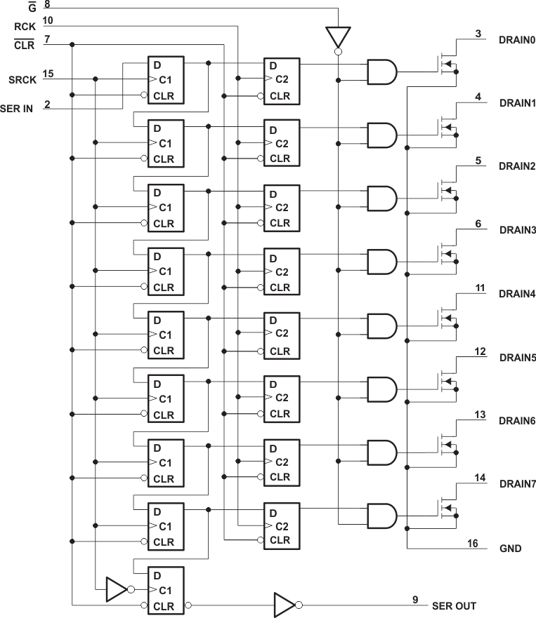
The TPIC6C596 device is a monolithic, medium-voltage,
low-current, 8-bit shift register designed for use in systems that require relatively moderate load
power such as LEDs. The device contains a built-in voltage clamp on the outputs for inductive
transient protection. Power driver applications include relays, solenoids, and other low-current or
medium-voltage loads.This device contains an 8-bit serial-in, parallel-out shift register that feeds an 8-bit
D-type storage register. Data transfers through both the shift and storage registers on the rising
edge of the shift register clock (SRCK) and the register clock (RCK), respectively. The storage
register transfers data to the output buffer when shift register clear (CLR)
is high. When CLR is low, all registers in the device are cleared. When
output enable (G) is held high, all data in the output buffers is held low
and all drain outputs are off. When G is held low, data from the storage
register is transparent to the output buffers. When data in the output buffers is low, the DMOS
transistor outputs are off. When data is high, the DMOS transistor outputs have sink-current
capability.The serial output (SER OUT) is clocked out of the device on the falling edge of SRCK to
provide additional hold time for cascaded applications. This will provide improved performance for
applications where clock signals may be skewed, devices are not located near one another, or the
system must tolerate electromagnetic interference.Outputs are low-side, open-drain DMOS transistors with output ratings of 33 V and 100 mA
continuous sink-current capability. Each output provides a 250-mA maximum current limit at
TC = 25°C. The current limit decreases as the junction temperature increases
for additional device protection. The device also provides up to 2500 V of ESD protection when
tested using the human body model and the 200-V machine model.The TPIC6C596 device is characterized for operation over the operating case temperature
range of –40°C to 125°C.
TPIC6C596PW 数据手册
| 数据手册 | 说明 | 数量 | 操作 |
|---|---|---|---|
 TPIC6C596PW TPIC6C596PW
|
IC PWR 8-BIT SHIFT REGIS 16TSSOP |
30页,1.14M | 查看 |
TPIC6C596PW 电路图
TPIC6C596PW 电路图
TPIC6C596PW 相关产品
- 100336QC
- 74AC299SCX
- 74AHC164PW,118
- 74HC164PW,118
- 74HC165D,653
- 74HC4094PW,118
- 74HC595D,118
- 74HC595N,112
- 74HC597D,653
- 74HCT164D,653
- 74HCT165D,652
- 74HCT4015N,112
- 74HCT4094D,112
- 74HCT4094D,118
- 74HCT595N,112
- 74LV164D,118
- 74LV165PW,118
- 74LV595PW,112
- CD4014BE
- CD4014BM96
- CD4014BPWR
- CD4015BE
- CD4015BM96
- CD4015BM96G4
- CD4015BPWR
- CD40194BE
- CD4021BE
- CD4021BM96
- CD4021BM96E4
- CD4021BPWR