 搜索
搜索
 发布采购
发布采购
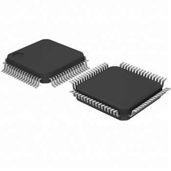
- 封装:64-LQFP
- RoHS:无铅 / 符合限制有害物质指令(RoHS)规范要求
- 包装方式:托盘
- 参考价格:$11-$9.9
更新日期:2024-04-01 00:04:00
产品简介:具有 18 位通用总线收发器的 3.3V ABT 扫描测试设备
查看详情- 封装:64-LQFP
- RoHS:无铅 / 符合限制有害物质指令(RoHS)规范要求
- 包装方式:托盘
- 参考价格:$11-$9.9
SN74LVTH18502APM 供应商
- 公司
- 型号
- 品牌
- 封装/批号
- 数量
- 地区
- 日期
- 说明
- 询价
-
TI
-
原厂原装
22+ -
3288
-
上海市
-
-
-
一级代理原装
-
TI
-
LQFP
2019+ -
5800
-
上海市
-
-
-
全新原装现货
-
TI(德州仪器)
-
LQFP-64(10x10)
2022+ -
12000
-
上海市
-
-
-
原装可开发票
SN74LVTH18502APM 中文资料属性参数
- 标准包装:160
- 类别:集成电路 (IC)
- 家庭:逻辑 - 专用逻辑
- 系列:74LVTH
- 逻辑类型:ABT 扫描测试设备,带通用总线收发器
- 电源电压:2.7 V ~ 3.6 V
- 位数:18
- 工作温度:-40°C ~ 85°C
- 安装类型:表面贴装
- 封装/外壳:64-LQFP
- 供应商设备封装:64-LQFP(10x10)
- 包装:托盘
- 其它名称:296-8699
产品特性
- Members of the Texas Instruments SCOPE™ Family of Testability Products
- Members of the Texas Instruments Widebus™ Family
- State-of-the-Art 3.3-V ABT Design Supports Mixed-Mode Signal Operation (5-V Input and Output Voltages With 3.3-V VCC)
- Support Unregulated Battery Operation Down to 2.7 V
- UBT™ (Universal Bus Transceiver) Combines D-Type Latches and D-Type Flip-Flops for Operation in Transparent, Latched, or Clocked Mode
- Bus Hold on Data Inputs Eliminates the Need for External Pullup Resistors
- B-Port Outputs of ’LVTH182502A Devices Have Equivalent 25- Series Resistors, So No External Resistors Are Required
- Compatible With the IEEE Standard 1149.1-1990 (JTAG) Test Access Port and Boundary-Scan Architecture
- SCOPE™ Instruction Set - IEEE Standard 1149.1-1990 Required Instructions and Optional CLAMP and HIGHZ - Parallel-Signature Analysis at Inputs - Pseudorandom Pattern Generation From Outputs - Sample Inputs/Toggle Outputs - Binary Count From Outputs - Device Identification - Even-Parity Opcodes
- Packaged in 64-Pin Plastic Thin Quad Flat (PM) Packages Using 0.5-mm Center-to-Center Spacings and 68-Pin Ceramic Quad Flat (HV) Packages Using 25-mil Center-to-Center Spacings
产品概述
The ’LVTH18502A and ’LVTH182502A scan test devices with 18-bit universal bus transceivers are members
of the Texas Instruments SCOPE™ testability integrated-circuit family. This family of devices supports IEEE
Standard 1149.1-1990 boundary scan to facilitate testing of complex circuit-board assemblies. Scan access to
the test circuitry is accomplished via the 4-wire test access port (TAP) interface.Additionally, these devices are designed specifically for low-voltage (3.3-V) VCC operation, but with the
capability to provide a TTL interface to a 5-V system environment.In the normal mode, these devices are 18-bit universal bus transceivers, that combine with D-type latches and
D-type flip-flops, they allow data to flow in the transparent, latched, or clocked modes. Another use is as two
9-bit transceivers or one 18-bit transceiver. The test circuitry can be activated by the TAP to take snapshot
samples of the data appearing at the device pins or to perform a self test on the boundary-test cells. Activating
the TAP in the normal mode does not affect the functional operation of the SCOPE universal bus transceivers.Data flow in each direction is controlled by output-enable (OEAB\ and OEBA\), latch-enable (LEAB and LEBA),
and clock (CLKAB and CLKBA) inputs. For A-to-B data flow, the device operates in the transparent mode when
LEAB is high. When LEAB is low, the A-bus data is latched while CLKAB is held at a static low or high logic level.
Otherwise, if LEAB is low, A-bus data is stored on a low-to-high transition of CLKAB. When OEAB\ is low, the
B outputs are active. When OEAB\ is high, the B outputs are in the high-impedance state. B-to-A data flow is
similar to A-to-B data flow, but uses the OEBA\, LEBA, and CLKBA inputs.In the test mode, the normal operation of the SCOPE universal bus transceivers is inhibited, and the test circuitry
is enabled to observe and control the I/O boundary of the device. When enabled, the test circuitry performs
boundary-scan test operations according to the protocol described in IEEE Standard 1149.1-1990.Four dedicated test pins are used to observe and control the operation of the test circuitry: test data input (TDI),
test data output (TDO), test mode select (TMS), and test clock (TCK). Additionally, the test circuitry performs
other testing functions such as parallel-signature analysis (PSA) on data inputs and pseudorandom pattern
generation (PRPG) from data outputs. All testing and scan operations are synchronized to the TAP interface.Active bus-hold circuitry is provided to hold unused or floating data inputs at a valid logic level.The B-port outputs of ’LVTH182502A, which are designed to source or sink up to 12 mA, include 25-
series resistors to reduce overshoot and undershoot.The SN54LVTH18502A and SN54LVTH182502A are characterized for operation over the full military
temperature range of –55°C to 125°C. The SN74LVTH18502A and SN74LVTH182502A are characterized for
operation from –40°C to 85°C.
SN74LVTH18502APM 数据手册
| 数据手册 | 说明 | 数量 | 操作 |
|---|---|---|---|
 SN74LVTH18502APM SN74LVTH18502APM
|
3.3-V ABT SCAN TEST DEVICES WITH 18-BIT UNIVERSAL BUS TRANSCEIVERS |
38 Pages页,614K | 查看 |
|
SN74LVTH18502APMG4
|
3.3-V ABT SCAN TEST DEVICES WITH 18-BIT UNIVERSAL BUS TRANSCEIVERS |
38 Pages页,614K | 查看 |
|
SN74LVTH18502APMR
|
3.3-V ABT SCAN TEST DEVICES WITH 18-BIT UNIVERSAL BUS TRANSCEIVERS |
38 Pages页,614K | 查看 |
|
SN74LVTH18502APMR
|
ABT Scan Test Device With Universal Bus Transceivers IC 64-LQFP (10x10) |
41页,843K | 查看 |
SN74LVTH18502APM 相关产品
- 74ACT1284MTCX
- 74LVC1GX04DCKTG4
- 74LVC1GX04GW,125
- 74SSTUB32868AZRHR
- 74SSTUB32868ZRHR
- 8V182512IDGGREP
- CD4007UBE
- CD4007UBEE4
- CD4007UBM96
- CD4007UBNSR
- CD4007UBPWR
- CD40117BE
- CD4089BE
- CD4089BEE4
- CD4089BNSR
- CD4089BPWR
- CD4527BE
- CD4527BNSR
- CD4527BPWR
- CD74AC283E
- CD74AC283M96
- CD74ACT283E
- CD74ACT283M
- CD74HC283E
- CD74HC283M
- CD74HC283M96
- CD74HCT283E
- CD74HCT283M96
- CLVC1GX04MDRLREP
- MC100E116FNR2G