 搜索
搜索
 发布采购
发布采购
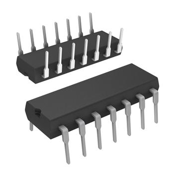
- 封装:14-DIP(0.300",7.62mm)
- RoHS:无铅 / 符合限制有害物质指令(RoHS)规范要求
- 包装方式:管件
- 参考价格:$0.47488-$1.3
更新日期:2024-04-01 00:04:00
产品简介:可编程双路 4 位终端控制器(20V 额定值)
查看详情- 封装:14-DIP(0.300",7.62mm)
- RoHS:无铅 / 符合限制有害物质指令(RoHS)规范要求
- 包装方式:管件
- 参考价格:$0.47488-$1.3
CD40117BE 供应商
- 公司
- 型号
- 品牌
- 封装/批号
- 数量
- 地区
- 日期
- 说明
- 询价
-
TI
-
原厂原装
22+ -
3288
-
上海市
-
-
-
一级代理原装
CD40117BE 中文资料属性参数
- 标准包装:25
- 类别:集成电路 (IC)
- 家庭:逻辑 - 专用逻辑
- 系列:4000B
- 逻辑类型:可编程端接器
- 电源电压:3 V ~ 18 V
- 位数:8
- 工作温度:-55°C ~ 125°C
- 安装类型:通孔
- 封装/外壳:14-DIP(0.300",7.62mm)
- 供应商设备封装:14-PDIP
- 包装:管件
- 其它名称:296-14244-5
产品特性
- One standard "B" output will drive eight terminator circuits.
- Will terminate a CMOS data bus with up to 40 B-series inputs inputs or 3-state outputs connected at VDD of 5 V.
- Input terminal protected by standard "B" series ESD protection network.
- Preserves final logic state.
- Output after switching is closer to VDD or VSS rail than with a resistor.
- Requires only one solder connection.
- Open circuited terminator not used will not affect performance.
- Can be connected to any CMOS I/O line.
- Draws current only when logic state is changing.
- Can be preset.
- Applications Error state identification. Replaces pull-up or pull-down resistors Avoids floating inputs in modular systems Sharpens transistors (hysteresis) Anti-bounce circuit
- Error state identification.
- Replaces pull-up or pull-down resistors
- Avoids floating inputs in modular systems
- Sharpens transistors (hysteresis)
- Anti-bounce circuit
产品概述
CD40117B is a dual 4-bit terminator that can be programmed by means of STROBE and DATA control bits to function as pull-up or pull-down resistors. The CD40117B can also be programmed to function as latches to terminate any open or unused CMOS logic when used with 3-state logic or during a power-down condition. Considerable savings in power and board space can be realized when this device is used to replace pull-up or pull-down resistors. When the STROBE is in the logic "1" state, the terminator functions as a pull-up resistor if the DATA input is a logic "1" or as a pull down resistor if the DATA input is a logic "0".When the STROBE is in the logic "0" state, the terminator performs the latch functions, i.e., it follows the changing states of the bus. If the bus goes into the high-Z state or into a power-down condition, the latched terminator retains the data ("1" or "0") that the bus carried before it switched to the high-Z or power-down state. If and when the bus changes from the high-Z state to the state opposite to that which the latch is storing, the bus will override the latch and the terminator will reflect the state on the bus. The small geometries chosen for the inverters in the latch allow this override mode. When checking the data bus whose last state is being preserved by the terminator, a resistor should be used in series with the probe whose input capacitance could trip the small latches. The resistance should be in excess of the output impedance of the latch, i.e., R should be > 30 K at VDD = 10 V.The STROBE and DATA inputs in each section can be paralleled allowing this device to be used as an 8-bit bus terminator.The CD40117B types are supplied in 14-lead dual-in-line plastic packages (E suffix), 14-lead small-outline packages
(M, MT, M96, and NSR suffixes), and 14-lead thin shrink small-outline packages (PW and PWR suffixes).
 CD40117BE
CD40117BE 相关产品
- 74ACT1284MTCX
- 74LVC1GX04DCKTG4
- 74LVC1GX04GW,125
- 74SSTUB32868AZRHR
- 74SSTUB32868ZRHR
- 8V182512IDGGREP
- CD4007UBE
- CD4007UBEE4
- CD4007UBM96
- CD4007UBNSR
- CD4007UBPWR
- CD4089BE
- CD4089BEE4
- CD4089BNSR
- CD4089BPWR
- CD4527BE
- CD4527BNSR
- CD4527BPWR
- CD74AC283E
- CD74AC283M96
- CD74ACT283E
- CD74ACT283M
- CD74HC283E
- CD74HC283M
- CD74HC283M96
- CD74HCT283E
- CD74HCT283M96
- CLVC1GX04MDRLREP
- MC100E116FNR2G
- MC100EP116MNG