 搜索
搜索
 发布采购
发布采购
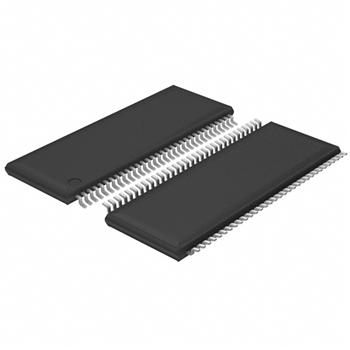
- 封装:64-TFSOP (0.240",6.10mm 宽)
- RoHS:无铅 / 符合限制有害物质指令(RoHS)规范要求
- 包装方式:Digi-Reel®
- 参考价格:$11.371-$18.84
更新日期:2024-04-01 00:04:00
产品简介:增强型产品,具有 18 位通用总线收发器的 3.3V Abt 扫描测试设备
查看详情- 封装:64-TFSOP (0.240",6.10mm 宽)
- RoHS:无铅 / 符合限制有害物质指令(RoHS)规范要求
- 包装方式:Digi-Reel®
- 参考价格:$11.371-$18.84
8V182512IDGGREP 供应商
- 公司
- 型号
- 品牌
- 封装/批号
- 数量
- 地区
- 日期
- 说明
- 询价
-
TI
-
原厂原装
22+ -
3288
-
上海市
-
-
-
一级代理原装
8V182512IDGGREP 中文资料属性参数
- 标准包装:1
- 类别:集成电路 (IC)
- 家庭:逻辑 - 专用逻辑
- 系列:-
- 逻辑类型:ABT 扫描测试设备,带通用总线收发器
- 电源电压:2.7 V ~ 3.6 V
- 位数:18
- 工作温度:-40°C ~ 85°C
- 安装类型:表面贴装
- 封装/外壳:64-TFSOP (0.240",6.10mm 宽)
- 供应商设备封装:64-TSSOP
- 包装:®
- 其它名称:296-22075-6
产品特性
- Controlled Baseline One Assembly/Test Site, One Fabrication Site
- One Assembly/Test Site, One Fabrication Site
- Enhanced Diminishing Manufacturing Sources (DMS) Support
- Enhanced Product-Change Notification
- Qualification Pedigree
- Members of the Texas Instruments SCOPE™ Family of Testability Products
- Members of the Texas Instruments Widebus™ Family
- State-of-the-Art 3.3-V ABT Design Supports Mixed-Mode Signal Operation (5-V Input and Output Voltages With 3.3-V VCC)
- Support Unregulated Battery Operation Down to 2.7 V
- UBT™ (Universal Bus Transceiver) Combines D-Type Latches and D-Type Flip-Flops for Operation in Transparent, Latched, or Clocked Mode
- Bus Hold on Data Inputs Eliminates the Need for External Pullup/Pulldown Resistors
- B-Port Outputs of SN74LVTH182512 Device Has Equivalent 25- Series Resistors, So No External Resistors Are Required
- SCOPE™ Instruction Set IEEE Std 1149.1-1990 Required Instructions and Optional CLAMP and HIGHZ Parallel-Signature Analysis at Inputs Pseudo-Random Pattern Generation From Outputs Sample Inputs/Toggle Outputs Binary Count From Outputs Device Identification Even-Parity Opcodes
- IEEE Std 1149.1-1990 Required Instructions and Optional CLAMP and HIGHZ
- Parallel-Signature Analysis at Inputs
- Pseudo-Random Pattern Generation From Outputs
- Sample Inputs/Toggle Outputs
- Binary Count From Outputs
- Device Identification
- Even-Parity Opcodes
- Compatible With the IEEE Std 1149.1-1990 (JTAG) Test Access Port and Boundary-Scan Architecture
产品概述
The SN74LVTH18512 and SN74LVTH182512 scan test devices with 18-bit universal bus transceivers are members of the Texas Instruments SCOPE™ testability integrated-circuit family. This family of devices supports IEEE Std 1149.1-1990 boundary scan to facilitate testing of complex circuit-board assemblies. Scan access to the test circuitry is accomplished via the 4-wire test access port (TAP) interface.Additionally, these devices are designed specifically for low-voltage (3.3-V) VCC operation, but with the capability to provide a TTL interface to a 5-V system environment.In the normal mode, these devices are 18-bit universal bus transceivers that combine D-type latches and D-type flip-flops to allow data flow in transparent, latched, or clocked modes. They can be used either as two 9-bit transceivers or one 18-bit transceiver. The test circuitry can be activated by the TAP to take snapshot samples of the data appearing at the device pins or to perform a self test on the boundary-test cells. Activating the TAP in the normal mode does not affect the functional operation of the SCOPE™ universal bus transceivers.Data flow in each direction is controlled by output-enable (OEAB\ and OEBA\), latch-enable (LEAB and LEBA), and clock (CLKAB and CLKBA) inputs. For A-to-B data flow, the devices operate in the transparent mode when LEAB is high. When LEAB is low, the A data is latched while CLKAB is held at a static low or high logic level. Otherwise, if LEAB is low, A data is stored on a low-to-high transition of CLKAB. When OEAB\ is low, the B outputs are active. When OEAB\ is high, the B outputs are in the high-impedance state. B-to-A data flow is similar to A-to-B data flow but uses the OEBA\, LEBA, and CLKBA inputs.In the test mode, the normal operation of the SCOPE™ universal bus transceivers is inhibited, and the test circuitry is enabled to observe and control the I/O boundary of the device. When enabled, the test circuitry performs boundary-scan test operations according to the protocol described in IEEE Std 1149.1-1990.Four dedicated test pins are used to observe and control the operation of the test circuitry: test data input (TDI), test data output (TDO), test mode select (TMS), and test clock (TCK). Additionally, the test circuitry performs other testing functions such as parallel-signature analysis (PSA) on data inputs and pseudo-random pattern generation (PRPG) from data outputs. All testing and scan operations are synchronized to the TAP interface.Active bus-hold circuitry is provided to hold unused or floating data inputs at a valid logic level.The B-port outputs of SN74LVTH182512, which are designed to source or sink up to 12 mA, include equivalent 25- series resistors to reduce overshoot and undershoot.
8V182512IDGGREP 数据手册
| 数据手册 | 说明 | 数量 | 操作 |
|---|---|---|---|
 8V182512IDGGREP 8V182512IDGGREP
|
ABT Scan Test Device With Universal Bus Transceivers IC 64-TSSOP |
38页,679K | 查看 |
8V182512IDGGREP 相关产品
- 74ACT1284MTCX
- 74LVC1GX04DCKTG4
- 74LVC1GX04GW,125
- 74SSTUB32868AZRHR
- 74SSTUB32868ZRHR
- CD4007UBE
- CD4007UBEE4
- CD4007UBM96
- CD4007UBNSR
- CD4007UBPWR
- CD40117BE
- CD4089BE
- CD4089BEE4
- CD4089BNSR
- CD4089BPWR
- CD4527BE
- CD4527BNSR
- CD4527BPWR
- CD74AC283E
- CD74AC283M96
- CD74ACT283E
- CD74ACT283M
- CD74HC283E
- CD74HC283M
- CD74HC283M96
- CD74HCT283E
- CD74HCT283M96
- CLVC1GX04MDRLREP
- MC100E116FNR2G
- MC100EP116MNG