 搜索
搜索
 发布采购
发布采购
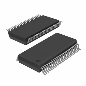
- 封装:48-TFSOP(0.240",6.10mm 宽)
- RoHS:无铅 / 符合限制有害物质指令(RoHS)规范要求
- 包装方式:Digi-Reel®
- 参考价格:$1.043-$2.23
更新日期:2024-04-01 00:04:00
产品简介:19 位 IEEE 1284 标准总线接口
查看详情- 封装:48-TFSOP(0.240",6.10mm 宽)
- RoHS:无铅 / 符合限制有害物质指令(RoHS)规范要求
- 包装方式:Digi-Reel®
- 参考价格:$1.043-$2.23
SN74LVCZ161284AGR 供应商
- 公司
- 型号
- 品牌
- 封装/批号
- 数量
- 地区
- 日期
- 说明
- 询价
-
TI
-
原厂原装
22+ -
3288
-
上海市
-
-
-
一级代理原装
-
TI(德州仪器)
-
TSSOP-48
2022+ -
12000
-
上海市
-
-
-
原装可开发票
-
TI
-
TSSOP
23+ -
46000
-
合肥
-
-
-
科大讯飞战略投资企业,提供一站式配套服务
SN74LVCZ161284AGR 中文资料属性参数
- 标准包装:1
- 类别:集成电路 (IC)
- 家庭:逻辑 - 专用逻辑
- 系列:74LVCZ
- 逻辑类型:IEEE STD 1284 转换收发器
- 电源电压:3 V ~ 3.6 V
- 位数:19
- 工作温度:0°C ~ 70°C
- 安装类型:表面贴装
- 封装/外壳:48-TFSOP(0.240",6.10mm 宽)
- 供应商设备封装:48-TSSOP
- 包装:®
- 其它名称:296-12025-6
产品特性
- Power-On Reset (POR) Prevents Printer Errors When Printer Is Turned On, But No Valid Signal Is at Pins A9–A13
- Operates From 3 V to 3.6 V
- 1.4-k Pullup Resistors Integrated on All Open-Drain Outputs Eliminate the Need for Discrete Resistors
- Designed for the IEEE Std 1284-I (Level-1 Type) and IEEE Std 1284-II (Level-2 Type) Electrical Specifications
- Flow-Through Architecture Optimizes PCB Layout
- Ioff and Power-Up 3-State Support Hot Insertion
- Latch-Up Performance Exceeds 100 mA Per JESD 78, Class II
- ESD Protection Exceeds JESD 22 4000-V Human-Body Model (A114-A) 350-V Machine Model (A115-A) 1500-V Charged-Device Model (C101)
- 4000-V Human-Body Model (A114-A)
- 350-V Machine Model (A115-A)
- 1500-V Charged-Device Model (C101)
产品概述
The SN74LVCZ161284A is designed for 3-V to 3.6-V VCC operation. This device provides asynchronous two-way communication between data buses. The control-function implementation minimizes external timing requirements.This device has eight bidirectional bits; data can flow in the A-to-B direction when the direction-control input (DIR) is high, and in the B-to-A direction when DIR is low. This device also has five drivers that drive the cable side, and four receivers. The SN74LVCZ161284A has one receiver dedicated to the HOST LOGIC line and a driver to drive the PERI LOGIC line.The output drive mode is determined by the high-drive (HD) control pin. When HD is high, the outputs are in a totem-pole configuration, and in an open-drain configuration when HD is low. This meets the drive requirements as specified in the IEEE Std 1284-I (level-1 type) and IEEE Std 1284-II (level-2 type) parallel peripheral-interface specifications. Except for HOST LOGIC IN and peripheral logic out (PERI LOGIC OUT), all cable-side pins have a 1.4-k integrated pullup resistor. The pullup resistor is switched off if the associated output driver is in the low state or if the output voltage is above VCC CABLE. If VCC CABLE is off, PERI LOGIC OUT is set to low.The device has two supply voltages. VCC is designed for 3-V to 3.6-V operation. VCC CABLE supplies the inputs and output buffers of the cable side only and is designed for 3-V to 3.6-V and for 4.7-V to 5.5-V operation. Even when VCC CABLE is 3 V to 3.6 V, the cable-side I/O pins are 5-V tolerant.The Power-On Reset (POR) ensures that the Y outputs (Y9–Y13) stay in the high state after power on until an associated input (A9–A13) goes high. When an associated input goes high, all Y outputs are activated, and noninverting signals of the associated inputs are driven through Y outputs. This special feature prevents printer system errors caused by deasserting the BUSY signal in the cable at power on.
SN74LVCZ161284AGR 数据手册
| 数据手册 | 说明 | 数量 | 操作 |
|---|---|---|---|
 SN74LVCZ161284AGR SN74LVCZ161284AGR
|
19-BIT IEEE 1284 TRANSLATION TRANSCEIVER WITH ERROR-FREE POWER UP |
10 Pages页,160K | 查看 |
|
SN74LVCZ161284AGR
|
IEEE STD 1284 Translation Transceiver IC 48-TSSOP |
13页,315K | 查看 |
SN74LVCZ161284AGR 相关产品
- 74ACT1284MTCX
- 74LVC1GX04DCKTG4
- 74LVC1GX04GW,125
- 74SSTUB32868AZRHR
- 74SSTUB32868ZRHR
- 8V182512IDGGREP
- CD4007UBE
- CD4007UBEE4
- CD4007UBM96
- CD4007UBNSR
- CD4007UBPWR
- CD40117BE
- CD4089BE
- CD4089BEE4
- CD4089BNSR
- CD4089BPWR
- CD4527BE
- CD4527BNSR
- CD4527BPWR
- CD74AC283E
- CD74AC283M96
- CD74ACT283E
- CD74ACT283M
- CD74HC283E
- CD74HC283M
- CD74HC283M96
- CD74HCT283E
- CD74HCT283M96
- CLVC1GX04MDRLREP
- MC100E116FNR2G