 搜索
搜索
 发布采购
发布采购
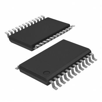
- 封装:24-TSSOP(0.173",4.40mm 宽)
- RoHS:无铅 / 符合限制有害物质指令(RoHS)规范要求
- 包装方式:Digi-Reel®
- 参考价格:$0.713-$1.66
更新日期:2024-04-01 00:04:00
产品简介:具有三态输出的八通道总线收发器和寄存器
查看详情- 封装:24-TSSOP(0.173",4.40mm 宽)
- RoHS:无铅 / 符合限制有害物质指令(RoHS)规范要求
- 包装方式:Digi-Reel®
- 参考价格:$0.713-$1.66
SN74LVC646APWR 供应商
- 公司
- 型号
- 品牌
- 封装/批号
- 数量
- 地区
- 日期
- 说明
- 询价
-
TI
-
原厂原装
22+ -
3288
-
上海市
-
-
-
一级代理原装
-
TI(德州仪器)
-
TSSOP-24
2022+ -
12000
-
上海市
-
-
-
原装可开发票
SN74LVC646APWR 中文资料属性参数
- 标准包装:1
- 类别:集成电路 (IC)
- 家庭:逻辑 - 缓冲器,驱动器,接收器,收发器
- 系列:74LVC
- 逻辑类型:收发器,非反相
- 元件数:1
- 每个元件的位元数:8
- 输出电流高,低:24mA,24mA
- 电源电压:1.65 V ~ 3.6 V
- 工作温度:-40°C ~ 85°C
- 安装类型:表面贴装
- 封装/外壳:24-TSSOP(0.173",4.40mm 宽)
- 供应商设备封装:24-TSSOP
- 包装:®
- 其它名称:296-8535-6
产品特性
- Operate From 1.65 V to 3.6 V
- Inputs Accept Voltages to 5.5 V
- Max tpd of 7.4 ns at 3.3 V
- Typical VOLP(Output Ground Bounce) <0.8 V at VCC = 3.3 V, TA = 25°C
- Typical VOHV (Output VOH Undershoot) >2 V at VCC = 3.3 V, TA = 25°C
- Supports Mixed-Mode Signal Operation on All Ports (5-V Input/Output Voltage With 3.3-V VCC)
- Ioff Supports Partial-Power-Down Mode Operation
- Latch-Up Performance Exceeds 250 mA Per JESD 17
- ESD Protection Exceeds JESD 22 2000-V Human-Body Model (A114-A) 200-V Machine Model (A115-A) 1000-V Charged-Device Model (C101)
- 2000-V Human-Body Model (A114-A)
- 200-V Machine Model (A115-A)
- 1000-V Charged-Device Model (C101)
产品概述
The SN54LVC646A octal bus transceiver and register is designed for 2.7-V to 3.6-V VCC operation, and the SN74LVC646A octal bus transceiver and register is designed for 1.65-V to 3.6-V VCC operation.These devices consist of bus-transceiver circuits, D-type flip-flops, and control circuitry arranged for multiplexed transmission of data directly from the input bus or from the internal registers. Data on the A or B bus is clocked into the registers on the low-to-high transition of the appropriate clock (CLKAB or CLKBA) input. Figure 1 illustrates the four fundamental bus-management functions that are performed with the ’LVC646A devices.Output-enable (OE)\ and direction-control (DIR) inputs control the transceiver functions. In the transceiver mode, data present at thehigh-impedance port is stored in either register or in both.The select-control (SAB and SBA) inputs can multiplex stored and real-time (transparent mode) data. DIR determines which bus receives data when OE\ is low. In the isolation mode (OE\ high), A data is stored in one register and B data can be stored in the other register.When an output function is disabled, the input function is still enabled and can be used to store and transmit data. Only one of the two buses, A or B, can be driven at a time.Inputs can be driven from either 3.3-V or 5-V devices. This feature allows the use of these devices as translators in a mixed 3.3-V/5-V system environment.These devices are fully specified for partial-power-down applications using Ioff. The Ioff circuitry disables the outputs, preventing damaging current backflow through the device when it is powered down.To ensure the high-impedance state during power up or power down, OE\ should be tied to VCC through a pullup resistor; the minimum value of the resistor is determined by the current-sinking capability of the driver.
SN74LVC646APWR 数据手册
| 数据手册 | 说明 | 数量 | 操作 |
|---|---|---|---|
 SN74LVC646APWR SN74LVC646APWR
|
Transceiver, Non-Inverting 1 Element 8 Bit per Element Push-Pull Output 24-TSSOP |
20页,874K | 查看 |
SN74LVC646APWR 相关产品
- 100314QC
- 1P1G125QDCKRG4Q1
- 1P1G125QDCKRQ1
- 1P1G126QDBVRQ1
- 74ABT125PW,118
- 74ABT162244CSSX
- 74ABT162244DGGRG4
- 74ABT162245DLRG4
- 74ABT16245ADGGRG4
- 74ABT244D,623
- 74ABT245PW,118
- 74AC11244DBR
- 74AC11244DWR
- 74AC11244PWR
- 74AC11245DW
- 74AC11245DWR
- 74AC16244DGGR
- 74AC16244DL
- 74AC16244DLR
- 74AC16245DLR
- 74AC16652DL
- 74ACT11244DBR
- 74ACT11244DWR
- 74ACT11244PWR
- 74ACT11245DBR
- 74ACT11245DWR
- 74ACT11245NSR
- 74ACT11245PWR
- 74ACT16244DGGR
- 74ACT16244DLR