 搜索
搜索
 发布采购
发布采购
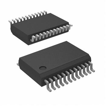
- 封装:24-SSOP(0.209",5.30mm 宽)
- RoHS:无铅 / 符合限制有害物质指令(RoHS)规范要求
- 包装方式:Digi-Reel®
- 参考价格:$0.66495-$1.55
更新日期:2024-04-01 00:04:00
产品简介:具有三态输出的八路寄存收发器
查看详情- 封装:24-SSOP(0.209",5.30mm 宽)
- RoHS:无铅 / 符合限制有害物质指令(RoHS)规范要求
- 包装方式:Digi-Reel®
- 参考价格:$0.66495-$1.55
SN74LVC543ADBR 供应商
- 公司
- 型号
- 品牌
- 封装/批号
- 数量
- 地区
- 日期
- 说明
- 询价
-
TI
-
原厂原装
22+ -
3288
-
上海市
-
-
-
一级代理原装
-
TI(德州仪器)
-
SSOP-24
2022+ -
12000
-
上海市
-
-
-
原装可开发票
SN74LVC543ADBR 中文资料属性参数
- 标准包装:1
- 类别:集成电路 (IC)
- 家庭:逻辑 - 缓冲器,驱动器,接收器,收发器
- 系列:74LVC
- 逻辑类型:寄存收发器,非反相
- 元件数:1
- 每个元件的位元数:8
- 输出电流高,低:24mA,24mA
- 电源电压:1.65 V ~ 3.6 V
- 工作温度:-40°C ~ 85°C
- 安装类型:表面贴装
- 封装/外壳:24-SSOP(0.209",5.30mm 宽)
- 供应商设备封装:24-SSOP
- 包装:®
- 其它名称:296-8522-6
产品特性
- Operates From 1.65 V to 3.6 V
- Inputs Accept Voltages to 5.5 V
- Max tpd of 7 ns at 3.3 V
- Typical VOLP (Output Ground Bounce) <0.8 V at VCC = 3.3 V, TA = 25°C
- Typical VOHV (Output VOH Undershoot) >2 V at VCC = 3.3 V, TA = 25°C
- Supports Mixed-Mode Signal Operation on All Ports (5-V Input/Output Voltage With 3.3-V VCC)
- Ioff Supports Partial-Power-Down Mode Operation
- Latch-Up Performance Exceeds 250 mA Per JESD 17
产品概述
This octal registered transceiver is designed for 1.65-V to 3.6-V VCC operation.The SN74LVC543A contains two sets of D-type latches for temporary storage of data flowing in either direction. Separate latch-enable (LEAB\ or LEBA\) and output-enable (OEAB\ or OEBA\) inputs are provided for each register to permit independent control in either direction of data flow.The A-to-B enable (CEAB)\ input must be low to enter data from A or to output data from B. If CEAB\ is low and LEAB\ is low, the A-to-B latches are transparent; a subsequent low-to-high transition of LEAB\ places the A latches in the storage mode. With CEAB\ and OEAB\ both low, the 3-state B outputs are active and reflect the data present at the output of the A latches. Data flow for B to A is similar to that of A to B, but uses CEBA\, LEBA\, and OEBA\.This device is fully specified for partial-power-down applications using Ioff. The Ioff circuitry disables the outputs, preventing damaging current backflow through the device when it is powered down.To ensure the high-impedance state during power up or power down, OE\ should be tied to VCC through a pullup resistor; the minimum value of the resistor is determined by the current-sinking capability of the driver.Inputs can be driven from either 3.3-V or 5-V devices. This feature allows the use of these devices as translators in a mixed 3.3-V/5-V system environment.
SN74LVC543ADBR 数据手册
| 数据手册 | 说明 | 数量 | 操作 |
|---|---|---|---|
 SN74LVC543ADBR SN74LVC543ADBR
|
Transceiver, Non-Inverting 1 Element 8 Bit per Element Push-Pull Output 24-SSOP |
16页,818K | 查看 |
SN74LVC543ADBR 相关产品
- 100314QC
- 1P1G125QDCKRG4Q1
- 1P1G125QDCKRQ1
- 1P1G126QDBVRQ1
- 74ABT125PW,118
- 74ABT162244CSSX
- 74ABT162244DGGRG4
- 74ABT162245DLRG4
- 74ABT16245ADGGRG4
- 74ABT244D,623
- 74ABT245PW,118
- 74AC11244DBR
- 74AC11244DWR
- 74AC11244PWR
- 74AC11245DW
- 74AC11245DWR
- 74AC16244DGGR
- 74AC16244DL
- 74AC16244DLR
- 74AC16245DLR
- 74AC16652DL
- 74ACT11244DBR
- 74ACT11244DWR
- 74ACT11244PWR
- 74ACT11245DBR
- 74ACT11245DWR
- 74ACT11245NSR
- 74ACT11245PWR
- 74ACT16244DGGR
- 74ACT16244DLR