 搜索
搜索
 发布采购
发布采购
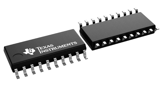
- 封装:20-SOIC(0.209",5.30mm 宽)
- RoHS:无铅 / 符合限制有害物质指令(RoHS)规范要求
- 包装方式:Digi-Reel®
- 参考价格:$0.4092-$0.95
更新日期:2024-04-01 00:04:00
产品简介:具有 TTL 兼容型 CMOS 输入和三态输出的 8 通道、4.5V 至 5.5V 缓冲器
查看详情- 封装:20-SOIC(0.209",5.30mm 宽)
- RoHS:无铅 / 符合限制有害物质指令(RoHS)规范要求
- 包装方式:Digi-Reel®
- 参考价格:$0.4092-$0.95
SN74LV541ATNSR 供应商
- 公司
- 型号
- 品牌
- 封装/批号
- 数量
- 地区
- 日期
- 说明
- 询价
-
TI
-
原厂原装
22+ -
3288
-
上海市
-
-
-
一级代理原装
SN74LV541ATNSR 中文资料属性参数
- 标准包装:1
- 类别:集成电路 (IC)
- 家庭:逻辑 - 缓冲器,驱动器,接收器,收发器
- 系列:74LV
- 逻辑类型:缓冲器/线路驱动器,非反相
- 元件数:1
- 每个元件的位元数:8
- 输出电流高,低:16mA,16mA
- 电源电压:4.5 V ~ 5.5 V
- 工作温度:-40°C ~ 85°C
- 安装类型:表面贴装
- 封装/外壳:20-SOIC(0.209",5.30mm 宽)
- 供应商设备封装:20-SO
- 包装:®
- 其它名称:296-28671-6
产品特性
- Inputs Are TTL-Voltage Compatible
- 4.5-V to 5.5-V VCC Operation
- Typical tpd of 4 ns at 5 V
- Typical VOLP (Output Ground Bounce) <0.8 V at VCC = 5 V, TA = 25°C
- Typical VOHV (Output VOH Undershoot) >2.3 V at VCC = 5 V, TA = 25°C
- Supports Mixed-Mode Voltage Operation on All Ports
- Ioff Supports Partial-Power-Down Mode Operation
- Latch-Up Performance Exceeds 250 mA Per JESD 17
- ESD Protection Exceeds JESD 22 2000-V Human-Body Model (A114-A) 200-V Machine Model (A115-A) 1000-V Charged-Device Model (C101)
- 2000-V Human-Body Model (A114-A)
- 200-V Machine Model (A115-A)
- 1000-V Charged-Device Model (C101)
产品概述
The SN74LV541AT is designed for 4.5-V to 5.5-V VCC operation. The
inputs are TTL-voltage compatible, which allows them to be interfaced with bipolar outputs and
3.3-V devices. The device also can be used to translate from 3.3 V to 5 V.This device is ideal for driving bus lines or buffer memory address registers. It
features inputs and outputs on opposite sides of the package to facilitate printed circuit board
layout.The 3-state control gate is a two-input AND gate with active-low inputs so that, if
either output-enable (OE1 or OE2) input is high, all
corresponding outputs are in the high-impedance state. The outputs provide noninverted data when
they are not in the high-impedance state.To ensure the high-impedance state during power up or power down,
OE shall be tied to VCC through a pullup resistor; the minimum value of the
resistor is determined by the current-sinking capability of the driver.This device is fully specified for partial-power-down applications using
Ioff. The Ioff circuitry disables the outputs,
preventing damaging current backflow through the device when it is powered down.
SN74LV541ATNSR 数据手册
| 数据手册 | 说明 | 数量 | 操作 |
|---|---|---|---|
 SN74LV541ATNSR SN74LV541ATNSR
|
Buffer, Non-Inverting 1 Element 8 Bit per Element Push-Pull Output 20-SO |
21页,1.24M | 查看 |
SN74LV541ATNSR 相关产品
- 100314QC
- 1P1G125QDCKRG4Q1
- 1P1G125QDCKRQ1
- 1P1G126QDBVRQ1
- 74ABT125PW,118
- 74ABT162244CSSX
- 74ABT162244DGGRG4
- 74ABT162245DLRG4
- 74ABT16245ADGGRG4
- 74ABT244D,623
- 74ABT245PW,118
- 74AC11244DBR
- 74AC11244DWR
- 74AC11244PWR
- 74AC11245DW
- 74AC11245DWR
- 74AC16244DGGR
- 74AC16244DL
- 74AC16244DLR
- 74AC16245DLR
- 74AC16652DL
- 74ACT11244DBR
- 74ACT11244DWR
- 74ACT11244PWR
- 74ACT11245DBR
- 74ACT11245DWR
- 74ACT11245NSR
- 74ACT11245PWR
- 74ACT16244DGGR
- 74ACT16244DLR