 搜索
搜索
 发布采购
发布采购
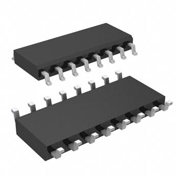
- 封装:16-SOIC(0.154",3.90mm 宽)
- RoHS:无铅 / 符合限制有害物质指令(RoHS)规范要求
- 包装方式:带卷 (TR)
- 参考价格:$0.4116
更新日期:2024-04-01 00:04:00
产品简介:串行输出移位寄存器
查看详情- 封装:16-SOIC(0.154",3.90mm 宽)
- RoHS:无铅 / 符合限制有害物质指令(RoHS)规范要求
- 包装方式:带卷 (TR)
- 参考价格:$0.4116
SN74LS166ADR 供应商
- 公司
- 型号
- 品牌
- 封装/批号
- 数量
- 地区
- 日期
- 说明
- 询价
-
TI
-
原厂原装
22+ -
3288
-
上海市
-
-
-
一级代理原装
-
TI
-
-
2019+ -
5800
-
上海市
-
-
-
全新原装现货
-
TI
-
SOP
23+ -
5800
-
上海市
-
-
-
进口原装现货,杜绝假货。
SN74LS166ADR 中文资料属性参数
- 标准包装:2,500
- 类别:集成电路 (IC)
- 家庭:逻辑 - 移位寄存器
- 系列:74LS
- 逻辑类型:移位寄存器
- 输出类型:标准
- 元件数:1
- 每个元件的位元数:8
- 功能:并行或串行至串行
- 电源电压:4.75 V ~ 5.25 V
- 工作温度:0°C ~ 70°C
- 安装类型:表面贴装
- 封装/外壳:16-SOIC(0.154",3.90mm 宽)
- 供应商设备封装:16-SOIC N
- 包装:带卷 (TR)
产品特性
- Synchronous Load
- Direct Overriding Clear
- Parallel to Serial Conversion
产品概述
The '166 and 'LS166A 8-bit shift registers are compatible with most other
TTL logic families. All '166 and 'LS166A inputs are buffered to lower the
drive requirements to one Series 54/74 or Series 54LS/74LS standard load,
respectively. Input clamping diodes minimize switching transients and simplify
system design.
These parallel-in or serial-in, serial-out shift registers have a complexity
of 77 equivalent gates on a monolithic chip. They feature gated clock inputs
and an overriding clear input. The parallel-in or serial-in modes are established
by the shift/load input. When high, this input enables the serial data input
and couples the eight flip-flops for serial shifting with each clock pulse.
When low, the parallel (broadside) data inputs are enabled and synchronous
loading occurs on the next clock pulse. During parallel loading, serial data
flow is inhibited. Clocking is accomplished on the low-to-high-level edge
of the clock pulse through a two-input positive NOR gate permitting one input
to be used as a clock-enable or clock-inhibit function. Holding either of
the clock inputs high inhibits clocking; holding either low enables the other
clock input. This, of course, allows the system clock to be free-running and
the register can be stopped on command with the other clock input. The clock
inhibit input should be changed to the high level only while the clock input
is high. A buffered, direct clear input overrides all other inputs, including
the clock, and sets all flip-flops to zero.
SN74LS166ADR 数据手册
| 数据手册 | 说明 | 数量 | 操作 |
|---|---|---|---|
 SN74LS166ADR SN74LS166ADR
|
PARALLEL-LOAD 8-BIT SHIFT REGISTERS |
16 Pages页,647K | 查看 |
|
SN74LS166ADRE4
|
PARALLEL-LOAD 8-BIT SHIFT REGISTERS |
16 Pages页,647K | 查看 |
SN74LS166ADR 相关产品
- 100336QC
- 74AC299SCX
- 74AHC164PW,118
- 74HC164PW,118
- 74HC165D,653
- 74HC4094PW,118
- 74HC595D,118
- 74HC595N,112
- 74HC597D,653
- 74HCT164D,653
- 74HCT165D,652
- 74HCT4015N,112
- 74HCT4094D,112
- 74HCT4094D,118
- 74HCT595N,112
- 74LV164D,118
- 74LV165PW,118
- 74LV595PW,112
- CD4014BE
- CD4014BM96
- CD4014BPWR
- CD4015BE
- CD4015BM96
- CD4015BM96G4
- CD4015BPWR
- CD40194BE
- CD4021BE
- CD4021BM96
- CD4021BM96E4
- CD4021BPWR