 搜索
搜索
 发布采购
发布采购
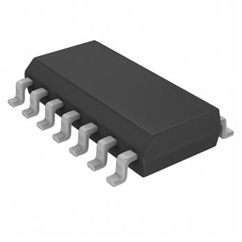
- 封装:14-SOIC(0.154",3.90mm 宽)
- RoHS:无铅 / 符合限制有害物质指令(RoHS)规范要求
- 包装方式:管件
- 参考价格:$0.34846-$0.92
更新日期:2024-04-01 00:04:00
产品简介:具有集电极开路输出的 6 通道、4.75V 至 5.25V 双极缓冲器
查看详情- 封装:14-SOIC(0.154",3.90mm 宽)
- RoHS:无铅 / 符合限制有害物质指令(RoHS)规范要求
- 包装方式:管件
- 参考价格:$0.34846-$0.92
SN74LS07D 供应商
- 公司
- 型号
- 品牌
- 封装/批号
- 数量
- 地区
- 日期
- 说明
- 询价
-
SN74LS07DR
订货 -
TI
-
SOP14
23+ -
9430
-
上海市
-
-
-
原装优势品牌
-
TI
-
TSSOP
23+ -
46000
-
合肥
-
-
-
科大讯飞战略投资企业,提供一站式配套服务
-
TI
-
-
2019+ -
5800
-
上海市
-
-
-
全新原装现货
-
TI(德州仪器)
-
SOIC-14
2022+ -
12000
-
上海市
-
-
-
原装可开发票
-
TI
-
SOP14
23+ -
15000
-
上海市
-
-
-
中国区代理原装现货热卖特价
-
TI
-
-
21+ -
2000
-
上海市
-
-
-
原装现货,品质为先!请来电垂询!
-
TI
-
-
4 -
5000
-
杭州
-
-
-
原装正品现货
-
TI
-
SSOP
23+ -
5800
-
上海市
-
-
-
进口原装现货,杜绝假货。
-
TI
-
14-SSOP
21+ -
10000
-
杭州
-
-
-
只做原装,大量现货供应
-
TI
-
-
22+ -
5000
-
常州
-
-
-
全新原装现货热卖
SN74LS07D 中文资料属性参数
- 标准包装:50
- 类别:集成电路 (IC)
- 家庭:逻辑 - 缓冲器,驱动器,接收器,收发器
- 系列:74LS
- 逻辑类型:缓冲器/线路驱动器,非反相
- 元件数:6
- 每个元件的位元数:1
- 输出电流高,低:40mA,40mA
- 电源电压:4.75 V ~ 5.25 V
- 工作温度:0°C ~ 70°C
- 安装类型:表面贴装
- 封装/外壳:14-SOIC(0.154",3.90mm 宽)
- 供应商设备封装:14-SOIC
- 包装:管件
- 其它名称:296-3626-5
产品特性
- Convert TTL Voltage Levels to MOS Levels
- High Sink-Current Capability
- Input Clamping Diodes Simplify System Design
- Open-Collector Driver for Indicator Lamps and Relays
产品概述
SN74LS07D 数据手册
| 数据手册 | 说明 | 数量 | 操作 |
|---|---|---|---|
 SN74LS07D SN74LS07D
|
Hex Buffers / Drivers with Open-Collector High-Vltage Outputs 14-SOIC 0 to 70 |
13页,506K | 查看 |
|
SN74LS07D
|
Buffer, Non-Inverting 6 Element 1 Bit per Element Open Collector Output 14-SOIC |
21页,1017K | 查看 |
|
SN74LS07DBR
|
Hex Buffers / Drivers with Open-Collector High-Vltage Outputs 14-SSOP 0 to 70 |
13页,506K | 查看 |
|
SN74LS07DR
|
Hex Buffers / Drivers with Open-Collector High-Vltage Outputs 14-SOIC 0 to 70 |
13页,506K | 查看 |
SN74LS07D 电路图

SN74LS07D 电路图
SN74LS07D 相关产品
- 100314QC
- 1P1G125QDCKRG4Q1
- 1P1G125QDCKRQ1
- 1P1G126QDBVRQ1
- 74ABT125PW,118
- 74ABT162244CSSX
- 74ABT162244DGGRG4
- 74ABT162245DLRG4
- 74ABT16245ADGGRG4
- 74ABT244D,623
- 74ABT245PW,118
- 74AC11244DBR
- 74AC11244DWR
- 74AC11244PWR
- 74AC11245DW
- 74AC11245DWR
- 74AC16244DGGR
- 74AC16244DL
- 74AC16244DLR
- 74AC16245DLR
- 74AC16652DL
- 74ACT11244DBR
- 74ACT11244DWR
- 74ACT11244PWR
- 74ACT11245DBR
- 74ACT11245DWR
- 74ACT11245NSR
- 74ACT11245PWR
- 74ACT16244DGGR
- 74ACT16244DLR