 搜索
搜索
 发布采购
发布采购
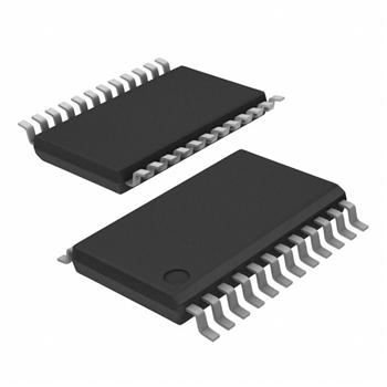
- 封装:24-TSSOP(0.173",4.40mm 宽)
- RoHS:无铅 / 符合限制有害物质指令(RoHS)规范要求
- 包装方式:管件
- 参考价格:$4.305
更新日期:2024-04-01 00:04:00
产品简介:GTLP 到 LVTTL 1 至 6 驱动器
查看详情- 封装:24-TSSOP(0.173",4.40mm 宽)
- RoHS:无铅 / 符合限制有害物质指令(RoHS)规范要求
- 包装方式:管件
- 参考价格:$4.305
SN74GTLP817PW 供应商
- 公司
- 型号
- 品牌
- 封装/批号
- 数量
- 地区
- 日期
- 说明
- 询价
-
TI
-
原厂原装
22+ -
3288
-
上海市
-
-
-
一级代理原装
SN74GTLP817PW 中文资料属性参数
- 标准包装:60
- 类别:集成电路 (IC)
- 家庭:逻辑 - 变换器
- 系列:74GTLP
- 逻辑功能:变换器,双向
- 位数:6
- 输入类型:GTLP
- 输出类型:LVTTL
- 数据速率:-
- 通道数:1
- 输出/通道数目:6
- 差分 - 输入:输出:无/无
- 传输延迟(最大):4.2ns
- 电源电压:3.15 V ~ 3.45 V
- 工作温度:-40°C ~ 85°C
- 封装/外壳:24-TSSOP(0.173",4.40mm 宽)
- 供应商设备封装:24-TSSOP
- 包装:管件
产品特性
- OEC™ Circuitry Improves Signal Integrity and Reduces Electromagnetic Interference
- Bidirectional Interface Between GTLP Signal Levels and LVTTL Logic Levels
- GTLP-to-LVTTL 1-to-6 Fanout Driver
- LVTTL-to-GTLP 1-to-2 Fanout Driver
- LVTTL Interfaces Are 5-V Tolerant
- Medium-Drive GTLP Outputs (50 mA)
- Reduced-Drive LVTTL Outputs (\x9612 mA/12 mA)
- Variable Edge-Rate Control (ERC) Input Selects GTLP Rise and Fall Times for Optimal Data-Transfer Rate and Signal Integrity in Distributed Loads
- Ioff and Power-Up 3-State Support Hot Insertion
- Distributed VCC and GND Pins Minimize High-Speed Switching Noise
- Latch-Up Performance Exceeds 100 mA Per JESD 78, Class II
- ESD Protection Exceeds JESD 22 2000-V Human-Body Model (A114-A) 200-V Machine Model (A115-A) 1000-V Charged-Device Model (C101)
- 2000-V Human-Body Model (A114-A)
- 200-V Machine Model (A115-A)
- 1000-V Charged-Device Model (C101)
产品概述
The SN74GTLP817 is a medium-drive fanout driver that provides LVTTL-to-GTLP and GTLP-to-LVTTL
signal-level translation. The device provides a high-speed interface between cards operating at LVTTL logic
levels and a backplane operating at GTLP signal levels. High-speed (about three times faster than standard
TTL or LVTTL) backplane operation is a direct result of GTLP reduced output swing (<1 V), reduced input
threshold levels, improved differential input, and OEC™ circuitry. The improved GTLP OEC circuitry minimizes
bus settling time and has been designed and tested using several backplane models. The medium drive allows
incident-wave switching in heavily loaded backplanes with equivalent load impedance down to 19 . BO1 and
BO2 can be tied together to drive an equivalent load impedance down to 11 .
GTLP is the Texas Instruments (TI™) derivative of the Gunning Transceiver Logic (GTL) JEDEC standard
JESD 8-3. The ac specification of the SN74GTLP817 is given only at the preferred higher noise-margin GTLP,
but the user has the flexibility of using this device at either GTL (VTT = 1.2 V and V REF = 0.8 V) or GTLP
(VTT = 1.5 V and VREF = 1 V) signal levels.
Normally, the B port operates at GTLP signal levels. The A-port and control inputs operate at LVTTL logic levels
but are 5-V tolerant and are compatible with TTL and 5-V CMOS inputs. VREF is the B-port differential input
reference voltage.
GNDT is the TTL output ground, while GNDG is the GTLP output ground, and both may be separated from each
other for a quieter device.
This device is fully specified for hot-insertion applications using Ioff and power-up 3-state. The Ioff circuitry
disables the outputs, preventing damaging current backflow through the device when it is powered down. The
power-up 3-state circuitry places the outputs in the high-impedance state during power up and power down,
which prevents driver conflict.
This device features adjustable edge-rate control (ERC). Changing the ERC input voltage between GND and
VCC adjusts the B-port output rise and fall times. This allows the designer to optimize system data-transfer rate
and signal integrity to the backplane load. ERC automatically is selected to the same speed as alternate source
1-to-6 fanout drivers that use pin 18 for 3.3-V or 5-V VCC .
When VCC is between 0 and 1.5 V, the device is in the high-impedance state during power up or power down.
However, to ensure the high-impedance state above 1.5 V, the output-enable (OE\) input should be tied to VCC
through a pullup resistor; the minimum value of the resistor is determined by the current-sinking capability of
the driver.
SN74GTLP817PW 相关产品
- 100324QC
- 100324SC
- 100325QC
- 100395QC
- 74ALVC164245DGG:11
- 74ALVC164245DGGRE4
- 74ALVC164245DGGRG4
- 74ALVC164245DGGTE4
- 74ALVC164245DGGTG4
- 74ALVC164245DL,118
- 74ALVC164245DLG4
- 74ALVC164245DLRG4
- 74AVC16T245DGVRE4
- 74AVC4T245BQ,115
- 74AVC4T245DGVRE4
- 74AVC4T245PW,118
- 74AVC4T245QRGYRQ1
- 74AVC4T245RGYRG4
- 74AVC4T245RSVRG4
- 74AVC4T774RSVRG4
- 74AVC8T245BQ,118
- 74AVC8T245RHLRG4
- 74AVCA164245GRE4
- 74AVCAH164245ZQLR
- 74AVCB164245GRE4
- 74AVCBH164245ZQLR
- 74AVCH1T45DBVRE4
- 74AVCH1T45DBVRG4
- 74AVCH1T45DCKRE4
- 74AVCH1T45DCKRG4