 搜索
搜索
 发布采购
发布采购
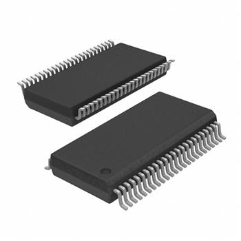
- 封装:48-TFSOP(0.240",6.10mm 宽)
- RoHS:无铅 / 符合限制有害物质指令(RoHS)规范要求
- 包装方式:带卷 (TR)
- 参考价格:$0.489
更新日期:2024-04-01 00:04:00
产品简介:具有三态输出的 16 位 2.5V 至 3.3V/3.3V 至 5V 电平转换收发器
查看详情- 封装:48-TFSOP(0.240",6.10mm 宽)
- RoHS:无铅 / 符合限制有害物质指令(RoHS)规范要求
- 包装方式:带卷 (TR)
- 参考价格:$0.489
74ALVC164245DGGRG4 供应商
- 公司
- 型号
- 品牌
- 封装/批号
- 数量
- 地区
- 日期
- 说明
- 询价
-
TI
-
原厂原装
22+ -
3288
-
上海市
-
-
-
一级代理原装
-
TI
-
TSSOP48
22+授权代理 -
15800
-
上海市
-
-
-
旋尔只做进口原装,假一赔十...
74ALVC164245DGGRG4 中文资料属性参数
- 标准包装:2,000
- 类别:集成电路 (IC)
- 家庭:逻辑 - 变换器
- 系列:74ALVC
- 逻辑功能:电平移位器,3 态
- 位数:16
- 输入类型:逻辑
- 输出类型:逻辑
- 数据速率:-
- 通道数:16
- 输出/通道数目:1
- 差分 - 输入:输出:无/无
- 传输延迟(最大):5.8ns
- 电源电压:2.3 V ~ 3.6 V ~ 3 V ~ 5.5 V
- 工作温度:-40°C ~ 85°C
- 封装/外壳:48-TFSOP(0.240",6.10mm 宽)
- 供应商设备封装:48-TSSOP
- 包装:带卷 (TR)
产品特性
- Member of the Texas Instruments Widebus™ Family
- Maximum tpd of 5.8 ns at 3.3 V
- ±24-mA Output Drive at 3.3 V
- Control Inputs VIH/VIL Levels Are Referenced to VCCA Voltage
- Latch-Up Performance Exceeds 250 mA Per JESD 17
- APPLICATIONS Electronic Points of Sale Printers and Other Peripherals Motor Drives Wireless and Telecom Infrastructures Wearable Health and Fitness Devices
- Electronic Points of Sale
- Printers and Other Peripherals
- Motor Drives
- Wireless and Telecom Infrastructures
- Wearable Health and Fitness Devices
产品概述
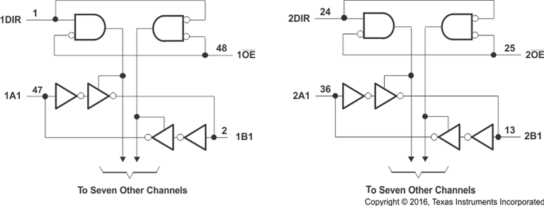
This 16-bit (dual-octal) noninverting bus transceiver contains two separate supply rails.
B port has VCCB, which is set to operate at 3.3 V and 5 V. A port has
VCCA, which is set to operate at 2.5 V and 3.3 V. This allows for
translation from a 2.5-V to a 3.3-V environment, and vice versa, or from a 3.3-V to a 5-V environment, and vice versa.The SN74ALVC164245 is designed for asynchronous communication between data buses. The
control circuitry (1DIR, 2DIR, 1OE, and 2OE) is powered by VCCA.To ensure the high-impedance state during power up or power down, the output-enable
(OE) input should be tied to VCC through a pullup
resistor; the minimum value of the resistor is determined by the current-sinking capability of the
driver.The logic levels of the direction-control (DIR) input and the output-enable
(OE) input activate either the B-port outputs or the A-port outputs or place
both output ports into the high-impedance mode. The device transmits data from the A bus to the B
bus when the B-port outputs are activated, and from the B bus to the A bus when the A-port outputs
are activated. The input circuitry on both A and B ports always is active and must have a logic
HIGH or LOW level applied to prevent excess ICC and
ICCZ.
74ALVC164245DGGRG4 电路图
74ALVC164245DGGRG4 电路图
74ALVC164245DGGRG4 相关产品
- 100324QC
- 100324SC
- 100325QC
- 100395QC
- 74ALVC164245DGG:11
- 74ALVC164245DGGRE4
- 74ALVC164245DGGTE4
- 74ALVC164245DGGTG4
- 74ALVC164245DL,118
- 74ALVC164245DLG4
- 74ALVC164245DLRG4
- 74AVC16T245DGVRE4
- 74AVC4T245BQ,115
- 74AVC4T245DGVRE4
- 74AVC4T245PW,118
- 74AVC4T245QRGYRQ1
- 74AVC4T245RGYRG4
- 74AVC4T245RSVRG4
- 74AVC4T774RSVRG4
- 74AVC8T245BQ,118
- 74AVC8T245RHLRG4
- 74AVCA164245GRE4
- 74AVCAH164245ZQLR
- 74AVCB164245GRE4
- 74AVCBH164245ZQLR
- 74AVCH1T45DBVRE4
- 74AVCH1T45DBVRG4
- 74AVCH1T45DCKRE4
- 74AVCH1T45DCKRG4
- 74AVCH4T245PWRG4