 搜索
搜索
 发布采购
发布采购
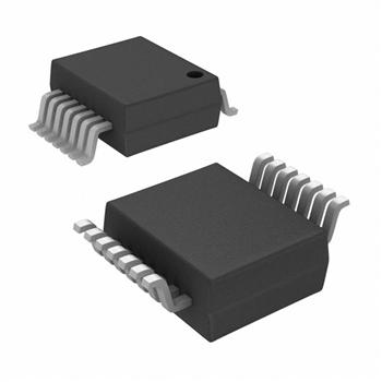
- 封装:16-TFSOP (0.173",4.40mm 宽)
- RoHS:无铅 / 符合限制有害物质指令(RoHS)规范要求
- 包装方式:Digi-Reel®
- 参考价格:$0.434-$1.01
更新日期:2024-04-01 00:04:00
产品简介:3.3V、8:1、单通道通用 FET 总线开关
- 封装:16-TFSOP (0.173",4.40mm 宽)
- RoHS:无铅 / 符合限制有害物质指令(RoHS)规范要求
- 包装方式:Digi-Reel®
- 参考价格:$0.434-$1.01
SN74CB3Q3251DGVR 供应商
- 公司
- 型号
- 品牌
- 封装/批号
- 数量
- 地区
- 日期
- 说明
- 询价
-
TI
-
原厂原装
22+ -
3288
-
上海市
-
-
-
一级代理原装
-
TI(德州仪器)
-
TVSOP-16
2022+ -
12000
-
上海市
-
-
-
原装可开发票
SN74CB3Q3251DGVR 中文资料属性参数
- 标准包装:1
- 类别:集成电路 (IC)
- 家庭:逻辑 - 信号开关,多路复用器,解码器
- 系列:74CB
- 类型:FET 多路复用器/多路分解器
- 电路:1 x 1:8
- 独立电路:1
- 输出电流高,低:15mA,30mA
- 电压电源:单电源
- 电源电压:2.3 V ~ 3.6 V
- 工作温度:-40°C ~ 85°C
- 安装类型:表面贴装
- 封装/外壳:16-TFSOP (0.173",4.40mm 宽)
- 供应商设备封装:16-TVSOP
- 包装:®
- 其它名称:296-19133-6
产品特性
- High-Bandwidth Data Path (up to 500 MHz (1))
- Equivalent to IDTQS3VH251 Device
- 5-V Tolerant I/Os With Device Powered Up or Powered Down
- Low and Flat ON-State Resistance (ron) Characteristics Over Operating Range (ron = 4 SN74CB3Q3251 的说明 The SN74CB3Q3251 is a high-bandwidth FET bus switch utilizing a charge pump to elevate the gate voltage of the pass transistor, providing a low and flat ON-state resistance (ron). The low and flat ON-state resistance allows for minimal propagation delay and supports rail-to-rail switching on the data input/output (I/O) ports. The device also features low data I/O capacitance to minimize capacitive loading and signal distortion on the data bus. Specifically designed to support high-bandwidth applications, the SN74CB3Q3251 provides an optimized interface solution ideally suited for broadband communications, networking, and data-intensive computing systems. The SN74CB3Q3251 is a 1-of-8 multiplexer/demultiplexer with a single output-enable (OE\) input. The select (S0, S1, S2) inputs control the data path of the multiplexer/demultiplexer. When OE\ is low, the multiplexer/demultiplexer is enabled, and the A port is connected to the B port, allowing bidirectional data flow between ports. When OE\ is high, the multiplexer/demultiplexer is disabled, and a high-impedance state exists between the A and B ports. This device is fully specified for partial-power-down applications using Ioff. The Ioff circuitry prevents damaging current backflow through the device when it is powered down. The device has isolation during power off. To ensure the high-impedance state during power up or power down, OE\ should be tied to VCC through a pullup resistor; the minimum value of the resistor is determined by the current-sinking capability of the driver.
SN74CB3Q3251DGVR 数据手册
| 数据手册 | 说明 | 数量 | 操作 |
|---|---|---|---|
 SN74CB3Q3251DGVR SN74CB3Q3251DGVR
|
1-OF-8 FET MULTIPLEXER/DEMULTIPLEXER 2.5-V/3.3-V LOW-VOLTAGE HIGH-BANDWIDTH BUS SWITCH |
1 Pages页,391K | 查看 |
|
SN74CB3Q3251DGVR
|
1-OF-8 FET MULTIPLEXER/DEMULTIPLEXER 2.5-V/3.3-V LOW-VOLTAGE, HIGH-BANDWIDTH BUS SWITCH |
12 Pages页,391K | 查看 |
|
SN74CB3Q3251DGVR
|
Multiplexer/Demultiplexer 1 x 8:1 16-TVSOP |
19页,990K | 查看 |
SN74CB3Q3251DGVR 相关产品
- 74AC11138D
- 74AC11138DR
- 74AC11138N
- 74AC11138NSR
- 74AC11138PWR
- 74AC11257DW
- 74AC11257N
- 74AC11257PW
- 74AC139MTCX
- 74ACT11139D
- 74ACT11139PWR
- 74ACT11257DWR
- 74ACT138SJX
- 74ACT139MTCX
- 74ACT139SCX
- 74ACT257SCX
- 74AHC138D,118
- 74CB3Q16244DGGRG4
- 74CB3Q3125DBQRE4
- 74CB3Q3245RGYRG4
- 74CB3Q3257DBQRE4
- 74CB3Q3257RGYRG4
- 74CB3Q3305DCURG4
- 74CB3Q3306ADCURE4
- 74CB3Q3306ADCURG4
- 74CB3T16210DGGRG4
- 74CB3T16211DGGRE4
- 74CB3T1G125DBVRE4
- 74CB3T1G125DBVRG4
- 74CB3T1G125DCKRG4