 搜索
搜索
 发布采购
发布采购
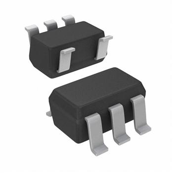
- 封装:SC-74A,SOT-753
- RoHS:无铅 / 符合限制有害物质指令(RoHS)规范要求
- 包装方式:带卷 (TR)
- 参考价格:$0.406
更新日期:2024-04-01 00:04:00
产品简介:具有电平转换器的 3.3V、1:1 (SPST)、单通道 FET 总线开关
查看详情- 封装:SC-74A,SOT-753
- RoHS:无铅 / 符合限制有害物质指令(RoHS)规范要求
- 包装方式:带卷 (TR)
- 参考价格:$0.406
74CB3T1G125DBVRE4 供应商
- 公司
- 型号
- 品牌
- 封装/批号
- 数量
- 地区
- 日期
- 说明
- 询价
-
TI
-
原厂原装
22+ -
3288
-
上海市
-
-
-
一级代理原装
74CB3T1G125DBVRE4 中文资料属性参数
- 标准包装:3,000
- 类别:集成电路 (IC)
- 家庭:逻辑 - 信号开关,多路复用器,解码器
- 系列:74CB
- 类型:FET 总线开关
- 电路:1 x 1:1
- 独立电路:1
- 输出电流高,低:-
- 电压电源:单电源
- 电源电压:2.3 V ~ 3.6 V
- 工作温度:-40°C ~ 85°C
- 安装类型:表面贴装
- 封装/外壳:SC-74A,SOT-753
- 供应商设备封装:SOT-23-5
- 包装:带卷 (TR)
产品特性
- Output Voltage Translation Tracks VCC
- Supports Mixed-Mode Signal Operation on All Data I/O Ports5-V Input Down to 3.3-V Output Level Shift With 3.3-V VCC5-V/3.3-V Input Down to 2.5-V Output Level Shift With 2.5-V VCC
- 5-V Input Down to 3.3-V Output Level Shift With 3.3-V VCC
- 5-V/3.3-V Input Down to 2.5-V Output Level Shift With 2.5-V VCC
- 5-V-Tolerant I/Os, With Device Powered Up or Powered Down
- Bidirectional Data Flow With Near-Zero Propagation Delay
- Low ON-State Resistance (ron) Characteristics (ron = 5 Typ)
- Low Input/Output Capacitance Minimizes Loading (Cio(OFF) = 5 pF Typ)
- Data and Control Inputs Provide Undershoot Clamp Diodes
- Low Power Consumption (ICC = 20 µA Max)
- VCC Operating Range From 2.3 V to 3.6 V
- Data I/Os Support 0- to 5-V Signaling Levels (0.8 V, 1.2 V, 1.5 V, 1.8 V, 2.5 V, 3.3 V, 5 V)
- Control Inputs Can Be Driven by TTL or 5-V/3.3-V CMOS Outputs
- Ioff Supports Partial-Power-Down Mode Operation
- Latch-Up Performance Exceeds 250 mA Per JESD 17
- ESD Performance Tested Per JESD 222000-V Human-Body Model (A114-B, Class II)1000-V Charged-Device Model (C101)
- 2000-V Human-Body Model (A114-B, Class II)
- 1000-V Charged-Device Model (C101)
- Supports Digital Applications: Level Translation, USB Interface, Bus Isolation
- Ideal for Low-Power Portable Equipment
产品概述
The SN74CB3T1G125 is a high-speed TTL-compatible FET bus switch with low ON-state resistance (ron), allowing for minimal propagation delay. The device fully supports mixed-mode signal operation on all data I/O ports by providing voltage translation that tracks VCC. The SN74CB3T1G125 supports systems using 5-V TTL, 3.3-V LVTTL, and 2.5-V CMOS switching standards, as well as user-defined switching levels.The SN74CB3T1G125 is a 1-bit bus switch with a single ouput-enable (OE) input. When OE is low, the bus switch is ON, and the A port is connected to the B port, allowing bidirectional data flow between ports. When OE is high, the bus switch is OFF, and a high-impedance state exists between the A and B ports.This device is fully specified for partial-power-down applications using Ioff. The Ioff feature ensures that damaging current will not backflow through the device when it is powered down. The device has isolation during power off.To ensure the high-impedance state during power up or power down, OE should be tied to VCC through a pullup resistor; the minimum value of the resistor is determined by the current-sinking capability of the driver.
74CB3T1G125DBVRE4 相关产品
- 74AC11138D
- 74AC11138DR
- 74AC11138N
- 74AC11138NSR
- 74AC11138PWR
- 74AC11257DW
- 74AC11257N
- 74AC11257PW
- 74AC139MTCX
- 74ACT11139D
- 74ACT11139PWR
- 74ACT11257DWR
- 74ACT138SJX
- 74ACT139MTCX
- 74ACT139SCX
- 74ACT257SCX
- 74AHC138D,118
- 74CB3Q16244DGGRG4
- 74CB3Q3125DBQRE4
- 74CB3Q3245RGYRG4
- 74CB3Q3257DBQRE4
- 74CB3Q3257RGYRG4
- 74CB3Q3305DCURG4
- 74CB3Q3306ADCURE4
- 74CB3Q3306ADCURG4
- 74CB3T16210DGGRG4
- 74CB3T16211DGGRE4
- 74CB3T1G125DBVRG4
- 74CB3T1G125DCKRG4
- 74CB3T3306DCURG4