 搜索
搜索
 发布采购
发布采购
- 封装:*
- RoHS:无铅 / 符合限制有害物质指令(RoHS)规范要求
- 包装方式:*
- 参考价格:$0.8568-$1.23
更新日期:2024-04-01 00:04:00
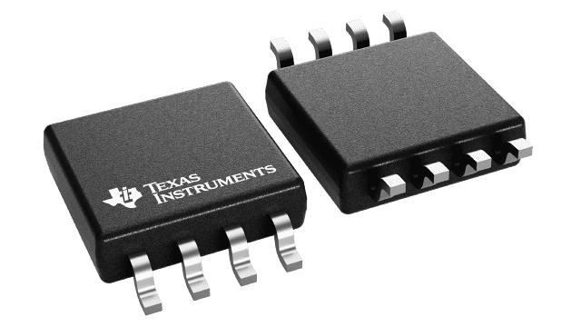
产品简介:具有可配置电压转换和三态输出的双位双电源总线收发器
查看详情- 封装:*
- RoHS:无铅 / 符合限制有害物质指令(RoHS)规范要求
- 包装方式:*
- 参考价格:$0.8568-$1.23
SN74AVC2T45DCTT 供应商
- 公司
- 型号
- 品牌
- 封装/批号
- 数量
- 地区
- 日期
- 说明
- 询价
-
TI
-
原厂原装
22+ -
3288
-
上海市
-
-
-
一级代理原装
-
TI(德州仪器)
-
SM8(SSOP)
2022+ -
12000
-
上海市
-
-
-
原装可开发票
SN74AVC2T45DCTT 中文资料属性参数
- 标准包装:1
- 类别:集成电路 (IC)
- 家庭:逻辑 - 变换器
- 系列:74AVC
- 逻辑功能:变换器,双向,3 态
- 位数:2
- 输入类型:逻辑
- 输出类型:逻辑
- 数据速率:500Mbps
- 通道数:2
- 输出/通道数目:1
- 差分 - 输入:输出:无/无
- 传输延迟(最大):2.4ns
- 电源电压:1.2 V ~ 3.6 V
- 工作温度:-40°C ~ 85°C
- 封装/外壳:*
- 供应商设备封装:*
- 包装:*
- 其它名称:296-32279-6
产品特性
- Available in the Texas Instruments NanoFree™ Package
- VCC Isolation Feature: If Either VCC Input Is at GND, Both Ports Are in the High-Impedance State
- Dual Supply Rail Design
- I/Os Are 4.6-V Over Voltage Tolerant
- Ioff Supports Partial-Power-Down Mode Operation
- Max Data Rates 500 Mbps (1.8 V to 3.3 V) 320 Mbps (<1.8 V to 3.3 V ) 320 Mbps (Level-Shifting to 2.5 V or 1.8 V) 280 Mbps (Level-Shifting to 1.5 V) 240 Mbps (Level-Shifting to 1.2 V)
- 500 Mbps (1.8 V to 3.3 V)
- 320 Mbps (<1.8 V to 3.3 V )
- 320 Mbps (Level-Shifting to 2.5 V or 1.8 V)
- 280 Mbps (Level-Shifting to 1.5 V)
- 240 Mbps (Level-Shifting to 1.2 V)
- Latch-Up Performance Exceeds 100 mA Per JESD 78, Class II
- ESD Protection Exceeds JESD 22
产品概述
This 2-bit non-inverting bus transceiver uses two separate configurable power-supply
rails. The A ports are designed to track VCCA and accepts any supply voltage
from 1.2 V to 3.6 V. The B ports are designed to track VCCB and accepts any
supply voltage from 1.2 V to 3.6 V. This allows for universal low-voltage bidirectional translation
and level-shifting between any of the 1.2-V, 1.5-V, 1.8-V, 2.5-V, and 3.3-V voltage nodes.The SN74AVC2T45 is designed for asynchronous communication between two data buses. The
logic levels of the direction-control (DIR pin) input activate either the B-port outputs or the
A-port outputs. The device transmits data from the A bus to the B bus when the B-port outputs are
activated and from the B bus to the A bus when the A-port outputs are activated. The input
circuitry on both A and B ports always is active and must have a logic HIGH or LOW level applied to
prevent excess leakage current on the internal CMOS structure.
SN74AVC2T45DCTT 数据手册
| 数据手册 | 说明 | 数量 | 操作 |
|---|---|---|---|
 SN74AVC2T45DCTT SN74AVC2T45DCTT
|
DUAL BIT DUAL SUPPLY BUS TRANSCEIVER WITH CONFIGURABLE VOLTAGE TRANSLATION AND 3 STATE OUTPUTS |
21 Pages页,377K | 查看 |
|
SN74AVC2T45DCTT
|
Voltage Level Translator Bidirectional 1 Circuit 2 Channel 500Mbps SM8 |
29页,976K | 查看 |
SN74AVC2T45DCTT 电路图
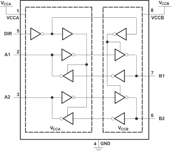
SN74AVC2T45DCTT 电路图
SN74AVC2T45DCTT 相关产品
- 100324QC
- 100324SC
- 100325QC
- 100395QC
- 74ALVC164245DGG:11
- 74ALVC164245DGGRE4
- 74ALVC164245DGGRG4
- 74ALVC164245DGGTE4
- 74ALVC164245DGGTG4
- 74ALVC164245DL,118
- 74ALVC164245DLG4
- 74ALVC164245DLRG4
- 74AVC16T245DGVRE4
- 74AVC4T245BQ,115
- 74AVC4T245DGVRE4
- 74AVC4T245PW,118
- 74AVC4T245QRGYRQ1
- 74AVC4T245RGYRG4
- 74AVC4T245RSVRG4
- 74AVC4T774RSVRG4
- 74AVC8T245BQ,118
- 74AVC8T245RHLRG4
- 74AVCA164245GRE4
- 74AVCAH164245ZQLR
- 74AVCB164245GRE4
- 74AVCBH164245ZQLR
- 74AVCH1T45DBVRE4
- 74AVCH1T45DBVRG4
- 74AVCH1T45DCKRE4
- 74AVCH1T45DCKRG4