 搜索
搜索
 发布采购
发布采购
- 封装:5-XFBGA,WLCSP
- RoHS:无铅 / 符合限制有害物质指令(RoHS)规范要求
- 包装方式:Digi-Reel®
- 参考价格:$0.2065-$0.58
更新日期:2024-04-01 00:04:00

产品简介:具有三态输出的单路 0.8V 至 3.6V 低功耗缓冲器
查看详情- 封装:5-XFBGA,WLCSP
- RoHS:无铅 / 符合限制有害物质指令(RoHS)规范要求
- 包装方式:Digi-Reel®
- 参考价格:$0.2065-$0.58
SN74AUP1G126YZPR 供应商
- 公司
- 型号
- 品牌
- 封装/批号
- 数量
- 地区
- 日期
- 说明
- 询价
-
TI
-
原厂原装
22+ -
3288
-
上海市
-
-
-
一级代理原装
-
TI(德州仪器)
-
DSBGA-5-5-WCSP(1.4x0.9)
2022+ -
12000
-
上海市
-
-
-
原装可开发票
SN74AUP1G126YZPR 中文资料属性参数
- 标准包装:1
- 类别:集成电路 (IC)
- 家庭:逻辑 - 缓冲器,驱动器,接收器,收发器
- 系列:74AUP
- 逻辑类型:缓冲器/线路驱动器,非反相
- 元件数:1
- 每个元件的位元数:1
- 输出电流高,低:4mA,4mA
- 电源电压:0.8 V ~ 3.6 V
- 工作温度:-40°C ~ 85°C
- 安装类型:表面贴装
- 封装/外壳:5-XFBGA,WLCSP
- 供应商设备封装:5-DSBGA,5-WCSP(1.4x0.9)
- 包装:®
- 其它名称:296-21014-6
产品特性
- Latch-Up Performance Exceeds 100 mA Per JESD 78, Class II
- ESD Performance Tested Per JESD 22− 2000-V Human-Body Model (A114-B, Class II) 1000-V Charged-Device Model (C101)
- 2000-V Human-Body Model (A114-B, Class II)
- 1000-V Charged-Device Model (C101)
- Available in the Texas Instruments NanoStar™ Package
- Low Static-Power Consumption (ICC = 0.9 µA Maximum)
- Low Dynamic-Power Consumption (Cpd = 4 pF Typical at 3.3 V)
- Low Input Capacitance (Ci = 1.5 pF Typical)
- Low Noise – Overshoot and Undershoot <10% of VCC
- Input-Disable Feature Allows Floating Input Conditions
- Ioff Supports Partial-Power-Down Mode Operation
- Input Hysteresis Allows Slow Input Transition and Better Switching Noise Immunity at Input
- Wide Operating VCC Range of 0.8 V to 3.6 V
- Optimized for 3.3-V Operation
- 3.6-V I/O Tolerant to Support Mixed-Mode Signal Operation
- tpd = 4.6 ns Maximum at 3.3 V
- Suitable for Point-to-Point Applications
产品概述
The AUP family is TI’s premier solution to the industry’s low-power needs in
battery-powered portable applications. This family assures a very low static and dynamic power
consumption across the entire VCC range of 0.8 V to 3.6 V, resulting in an
increased battery life. This product also maintains excellent signal integrity (see
AUP – The Lowest-Power Family and Excellent Signal Integrity ).This bus buffer gate is a single line driver with a 3-state output. The output is
disabled when the output-enable (OE) input is low. This device has the input-disable feature, which
allows floating input signals.To assure the high-impedance state during power up or power down, OE should be tied to
GND through a pulldown resistor; the minimum value of the resistor is determined by the
current-sourcing capability of the driver. NanoStar™ package technology is a major
breakthrough in IC packaging concepts, using the die as the package.This device is fully specified for partial-power-down applications using
Ioff. The Ioff circuitry disables the outputs when
the device is powered down. This inhibits current backflow into the device which prevents damage to
the device.
SN74AUP1G126YZPR 数据手册
| 数据手册 | 说明 | 数量 | 操作 |
|---|---|---|---|
 SN74AUP1G126YZPR SN74AUP1G126YZPR
|
LOW-POWER SINGLE BUS BUFFER GATE WITH 3-STATS OUTPUT |
17 Pages页,367K | 查看 |
|
SN74AUP1G126YZPR
|
Buffer, Non-Inverting 1 Element 1 Bit per Element Push-Pull Output 5-DSBGA, 5-WCSP (1.4x0.9) |
31页,1.37M | 查看 |
SN74AUP1G126YZPR 电路图
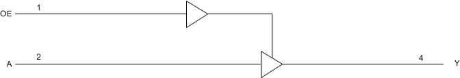
SN74AUP1G126YZPR 电路图
SN74AUP1G126YZPR 相关产品
- 100314QC
- 1P1G125QDCKRG4Q1
- 1P1G125QDCKRQ1
- 1P1G126QDBVRQ1
- 74ABT125PW,118
- 74ABT162244CSSX
- 74ABT162244DGGRG4
- 74ABT162245DLRG4
- 74ABT16245ADGGRG4
- 74ABT244D,623
- 74ABT245PW,118
- 74AC11244DBR
- 74AC11244DWR
- 74AC11244PWR
- 74AC11245DW
- 74AC11245DWR
- 74AC16244DGGR
- 74AC16244DL
- 74AC16244DLR
- 74AC16245DLR
- 74AC16652DL
- 74ACT11244DBR
- 74ACT11244DWR
- 74ACT11244PWR
- 74ACT11245DBR
- 74ACT11245DWR
- 74ACT11245NSR
- 74ACT11245PWR
- 74ACT16244DGGR
- 74ACT16244DLR