 搜索
搜索
 发布采购
发布采购
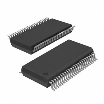
- 封装:48-TFSOP(0.240",6.10mm 宽)
- RoHS:无铅 / 符合限制有害物质指令(RoHS)规范要求
- 包装方式:Digi-Reel®
- 参考价格:$1.656-$3.31
更新日期:2024-04-01 00:04:00
产品简介:具有 4 个独立缓冲器的 8 位总线收发器和透明 D 类锁存器
查看详情- 封装:48-TFSOP(0.240",6.10mm 宽)
- RoHS:无铅 / 符合限制有害物质指令(RoHS)规范要求
- 包装方式:Digi-Reel®
- 参考价格:$1.656-$3.31
SN74ALVCH16973DGGR 供应商
- 公司
- 型号
- 品牌
- 封装/批号
- 数量
- 地区
- 日期
- 说明
- 询价
-
TI
-
原厂原装
22+ -
3288
-
上海市
-
-
-
一级代理原装
-
TI(德州仪器)
-
TSSOP-48
2022+ -
12000
-
上海市
-
-
-
原装可开发票
SN74ALVCH16973DGGR 中文资料属性参数
- 标准包装:1
- 类别:集成电路 (IC)
- 家庭:逻辑 - 缓冲器,驱动器,接收器,收发器
- 系列:74ALVCH
- 逻辑类型:收发器,非反相
- 元件数:1
- 每个元件的位元数:8
- 输出电流高,低:24mA,24mA
- 电源电压:1.65 V ~ 3.6 V
- 工作温度:-40°C ~ 85°C
- 安装类型:表面贴装
- 封装/外壳:48-TFSOP(0.240",6.10mm 宽)
- 供应商设备封装:48-TSSOP
- 包装:®
- 其它名称:296-15397-6
产品特性
- Member of the Texas Instruments Widebus™ Family
- Bus Hold on Data Inputs Eliminates the Need for External Pullup/Pulldown Resistors
- Latch-Up Performance Exceeds 250 mA Per JESD 17
- ESD Protection Exceeds JESD 22 2000-V Human-Body Model (A114-A) 200-V Machine Model (A115-A) 1000-V Charged-Device Model (C101)
- 2000-V Human-Body Model (A114-A)
- 200-V Machine Model (A115-A)
- 1000-V Charged-Device Model (C101)
产品概述
This device contains four independent noninverting buffers and an 8-bit noninverting bus transceiver and D-type latch, designed for 1.65-V to 3.6-V VCC operation.The SN74ALVCH16973 is particularly suitable for demultiplexing an address/data bus into a dedicated address bus and dedicated data bus. The device is used where there is asynchronous bidirectional communication between the A and B data bus, and the address signals are latched and buffered on the Q bus. The control-function implementation minimizes external timing requirements.This device can be used as one 4-bit buffer, one 8-bit transceiver, and one 8-bit latch. It allows data transmission from the A bus to the B bus or from the B bus to the A bus, depending on the logic level at the direction-control (DIR) input. The transceiver output-enable (TOE)\ input can be used to disable the transceivers so that the A and B buses effectively are isolated.When the latch-enable (LE) input is high, the Q outputs follow the data (A) inputs. When LE is taken low, the Q outputs are latched at the levels set up at the A inputs. The latch output-enable (LOE)\ input can be used to place the nine Q outputs in either a normal logic state (high or low logic level) or the high-impedance state. In the high-impedance state, the Q outputs neither drive nor load the bus lines significantly. LOE\ does not affect internal operations of the latch. Old data can be retained or new data can be entered while the Q outputs are in the high-impedance state.To ensure the high-impedance state during power up or power down, LOE\ and TOE\ should be tied to VCC through pullup resistors; the minimum values of the resistors are determined by the current-sinking capability of the drivers.The four independent noninverting buffers perform the Boolean function Y = D and are independent of the state of DIR, TOE\, LE, and LOE\.The A and B I/Os, and D inputs have bus-hold circuitry. Active bus-hold circuitry holds unused or undriven data inputs at a valid logic state. Use of pullup or pulldown resistors with the bus-hold circuitry is not recommended.
SN74ALVCH16973DGGR 数据手册
| 数据手册 | 说明 | 数量 | 操作 |
|---|---|---|---|
 SN74ALVCH16973DGGR SN74ALVCH16973DGGR
|
Transceiver, Non-Inverting 1 Element 8 Bit per Element Push-Pull Output 48-TSSOP |
14页,671K | 查看 |
SN74ALVCH16973DGGR 相关产品
- 100314QC
- 1P1G125QDCKRG4Q1
- 1P1G125QDCKRQ1
- 1P1G126QDBVRQ1
- 74ABT125PW,118
- 74ABT162244CSSX
- 74ABT162244DGGRG4
- 74ABT162245DLRG4
- 74ABT16245ADGGRG4
- 74ABT244D,623
- 74ABT245PW,118
- 74AC11244DBR
- 74AC11244DWR
- 74AC11244PWR
- 74AC11245DW
- 74AC11245DWR
- 74AC16244DGGR
- 74AC16244DL
- 74AC16244DLR
- 74AC16245DLR
- 74AC16652DL
- 74ACT11244DBR
- 74ACT11244DWR
- 74ACT11244PWR
- 74ACT11245DBR
- 74ACT11245DWR
- 74ACT11245NSR
- 74ACT11245PWR
- 74ACT16244DGGR
- 74ACT16244DLR