 搜索
搜索
 发布采购
发布采购
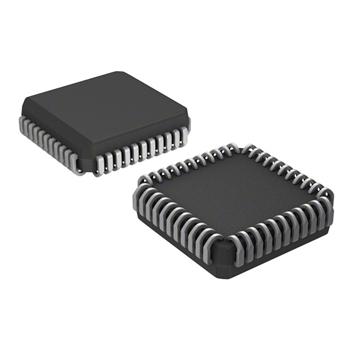
- 封装:44-LCC(J 形引线)
- RoHS:无铅 / 符合限制有害物质指令(RoHS)规范要求
- 包装方式:Digi-Reel®
- 参考价格:$26.82-$37.08
更新日期:2024-04-01 00:04:00
产品简介:具有 16 位通用主机接口的测试总线控制器 IEEE Std 1149.1 (JTAG) TAP 主控方
查看详情- 封装:44-LCC(J 形引线)
- RoHS:无铅 / 符合限制有害物质指令(RoHS)规范要求
- 包装方式:Digi-Reel®
- 参考价格:$26.82-$37.08
SN74ACT8990FNR 供应商
- 公司
- 型号
- 品牌
- 封装/批号
- 数量
- 地区
- 日期
- 说明
- 询价
-
TI
-
原厂原装
22+ -
3288
-
上海市
-
-
-
一级代理原装
-
TI(德州仪器)
-
PLCC-44(16.58x16.58)
2022+ -
12000
-
上海市
-
-
-
原装可开发票
SN74ACT8990FNR 中文资料属性参数
- 标准包装:1
- 类别:集成电路 (IC)
- 家庭:逻辑 - 专用逻辑
- 系列:74ACT
- 逻辑类型:测试总线控制器
- 电源电压:4.5 V ~ 5.5 V
- 位数:16
- 工作温度:0°C ~ 70°C
- 安装类型:表面贴装
- 封装/外壳:44-LCC(J 形引线)
- 供应商设备封装:44-PLCC(16.59x16.59)
- 包装:®
- 其它名称:296-4505-6
产品特性
- Members of the Texas Instruments SCOPETM Family of Testability Products
- Compatible With the IEEE Standard 1149.1-1990 (JTAG) Test Access Port and Boundary-Scan Architecture
- Control Operation of Up to Six Parallel Target Scan Paths
- Accommodate Pipeline Delay to Target of Up to 31 Clock Cycles
- Scan Data Up to 232 Clock Cycles
- Execute Instructions for Up to 232 Clock Cycles
- Each Device Includes Four Bidirectional Event Pins for Additional Test Capability
- Inputs Are TTL-Voltage Compatible
- EPICTM (Enhanced-Performance Implanted CMOS) 1-m Process
- Packaged in 44-Pin Plastic Leaded Chip Carrier (FN), 68-Pin Ceramic Pin Grid Array (GB), and 68-Pin Ceramic Quad Flat Packages (HV) SCOPE and EPIC are trademarks of Texas Instruments Incorporated.
产品概述
The 'ACT8990 test-bus controllers (TBC) are members of the Texas
Instruments SCOPETM testability integrated-circuit family.
This family of components supports IEEE Standard 1149.1-1990 (JTAG)
boundary scan to facilitate testing of complex circuit-board
assemblies. The 'ACT8990 differ from other SCOPETM
integrated circuits. Their function is to control the JTAG
serial-test bus rather than being target boundary-scannable devices.
The required signals of the JTAG serial-test bus - test clock
(TCK), test mode select (TMS), test data input (TDI), and test data
output (TDO) can be connected from the TBC to a target device without
additional logic. This is done as a chain of IEEE Standard
1149.1-1990 boundary-scannable components that share the same
serial-test bus. The TBC generates TMS and TDI signals for its
target(s), receives TDO signals from its target(s), and buffers its
test clock input (TCKI) to a test clock output (TCKO) for
distribution to its target(s). The TMS, TDI, and TDO signals can be
connected to a target directly or via a pipeline, with a retiming
delay of up to 31 bits. Since the TBC can be configured to generate
up to six separate TMS signals [TMS (5-0)], it can be used to control
up to six target scan paths that are connected in parallel (i.e.,
sharing common TCK, TDI, and TDO signals).While most operations of the TBC are synchronous to TCKI, a
test-off (TOFF\) input is provided for output control of the target
interface, and a test-reset (TRST\) input is provided for
hardware/software reset of the TBC. In addition, four event [EVENT
(3-0)] I/Os are provided for asynchronous communication to target
device(s). Each event has its own event generation/detection logic,
and detected events can be counted by two 16-bit counters.The TBC operates under the control of a host
microprocessor/microcontroller via the 5-bit address bus [ADRS (4-0)]
and the 16-bit read/write data bus [DATA (15-0)]. Read (RD\) and
write (WR\) strobes are implemented such that the critical
host-interface timing is independent of the TCKI period. Any one of
24 registers can be addressed for read and/or write operations. In
addition to control and status registers, the TBC contains two
command registers, a read buffer, and a write buffer. Status of the
TBC is transmitted to the host via ready (RDY\) and interrupt (INT\)
outputs.Major commands can be issued by the host to cause the TBC to
generate the TMS sequences necessary to move the target(s) from any
stable test-access-port (TAP) controller state to any other stable
TAP state, to execute instructions in the Run-Test/Idle TAP state, or
to scan instruction or test data through the target(s). A 32-bit
counter can be preset to allow a predetermined number of execution or
scan operations.Serial data that appears at the selected TDI input (TDI1 or TDI0)
is transferred into the read buffer, which can be read by the host to
obtain up to 16 bits of the serial-data stream. Serial data that is
transmitted from the TDO output is written by the host to the write
buffer. The SN54ACT8990 is characterized for operation over the full
military temperature range of -55°C to 125°C. The
SN74ACT8990 is characterized for operation from 0°C to
70°C. NC - No internal connection
SN74ACT8990FNR 数据手册
| 数据手册 | 说明 | 数量 | 操作 |
|---|---|---|---|
 SN74ACT8990FNR SN74ACT8990FNR
|
TEST-BUS CONTROLLERS IEEE STD 1149.1 JTAG TAP MASTERS WITH 16-BIT GENERIC HOST INTERFACES |
15 Pages页,286K | 查看 |
SN74ACT8990FNR 相关产品
- 74ACT1284MTCX
- 74LVC1GX04DCKTG4
- 74LVC1GX04GW,125
- 74SSTUB32868AZRHR
- 74SSTUB32868ZRHR
- 8V182512IDGGREP
- CD4007UBE
- CD4007UBEE4
- CD4007UBM96
- CD4007UBNSR
- CD4007UBPWR
- CD40117BE
- CD4089BE
- CD4089BEE4
- CD4089BNSR
- CD4089BPWR
- CD4527BE
- CD4527BNSR
- CD4527BPWR
- CD74AC283E
- CD74AC283M96
- CD74ACT283E
- CD74ACT283M
- CD74HC283E
- CD74HC283M
- CD74HC283M96
- CD74HCT283E
- CD74HCT283M96
- CLVC1GX04MDRLREP
- MC100E116FNR2G