 搜索
搜索
 发布采购
发布采购
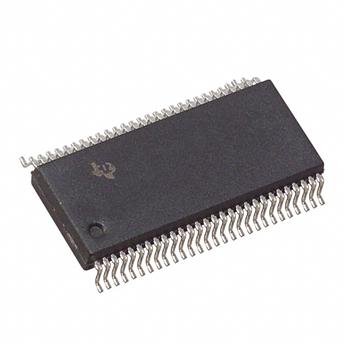
- 封装:56-BSSOP(0.295",7.50mm 宽)
- RoHS:无铅 / 符合限制有害物质指令(RoHS)规范要求
- 包装方式:管件
- 参考价格:$8.61
更新日期:2024-04-01 00:04:00
产品简介:64 x 18 同步 FIFO 存储器
查看详情- 封装:56-BSSOP(0.295",7.50mm 宽)
- RoHS:无铅 / 符合限制有害物质指令(RoHS)规范要求
- 包装方式:管件
- 参考价格:$8.61
SN74ACT7813-15DL 供应商
- 公司
- 型号
- 品牌
- 封装/批号
- 数量
- 地区
- 日期
- 说明
- 询价
-
TI
-
原厂原装
22+ -
3288
-
上海市
-
-
-
一级代理原装
-
TI
-
SSOP56
0 -
50
-
杭州
-
-
-
原装正品现货
-
TI
-
-
2019+ -
5800
-
上海市
-
-
-
全新原装现货
SN74ACT7813-15DL 中文资料属性参数
- 标准包装:20
- 类别:集成电路 (IC)
- 家庭:逻辑 - FIFO
- 系列:74ACT
- 功能:同步
- 存储容量:1.1K(64 x 18)
- 数据速率:67MHz
- 访问时间:-
- 电源电压:4.5 V ~ 5.5 V
- 工作温度:0°C ~ 70°C
- 安装类型:表面贴装
- 封装/外壳:56-BSSOP(0.295",7.50mm 宽)
- 供应商设备封装:56-SSOP
- 包装:管件
- 其它名称:296-4484-5
产品特性
- Member of the Texas Instruments WidebusTM Family
- Free-Running Read and Write Clocks Can Be Asynchronous or Coincident
- Read and Write Operations Synchronized to Independent System Clocks
- Input-Ready Flag Synchronized to Write Clock
- Output-Ready Flag Synchronized to Read Clock
- 64 Words by 18 Bits
- Low-Power Advanced CMOS Technology
- Half-Full Flag and Programmable Almost-Full/Almost-Empty Flag
- Bidirectional Configuration and Width Expansion Without Additional Logic
- Fast Access Times of 12 ns With a 50-pF Load and All Data Outputs Switching Simultaneously
- Data Rates up to 67 MHz
- Pin-to-Pin Compatible With SN74ACT7803 and SN74ACT7805
- Packaged in Shrink Small-Outline 300-mil Package Using 25-mil Center-to-Center Spacing Widebus and OEC are trademarks of Texas Instruments Incorporated.
产品概述
The SN74ACT7813 is a 64-word × 18-bit FIFO suited for buffering asynchronous datapaths up to 67-MHz clock rates and 12-ns access times. Two
devices can be configured for bidirectional data buffering without additional logic. Multiple distributed VCC and GND pins, along with Texas Instruments patented output edge control (OECTM) circuit, dampen simultaneous switching noise.
The write clock (WRTCLK) and read clock (RDCLK) are free running and can be asynchronous or coincident. Data is written to memory on the rising edge of WRTCLK when WRTEN1 is high, WRTEN2\ is low, and input ready (IR) is high. Data is read from memory on the rising edge of RDCLK when RDEN\, OE1\, and OE2\ are low and output ready (OR) is high. The first word written to memory is clocked through to the output buffer regardless of the RDEN\, OE1\, and OE2\ levels. The OR flag indicates that valid data is present on the output buffer.
The FIFO can be reset asynchronously to WRTCLK and RDCLK. RESET\ must be asserted while at least four WRTCLK and four RDCLK rising edges occur to clear the synchronizing registers. Resetting the FIFO initializes the IR, OR, and half-full (HF) flags low and the almost-full/almost-empty (AF/AE) flag high. The FIFO must be reset upon power up.
The SN74ACT7813 is characterized for operation from 0°C to 70°C.
SN74ACT7813-15DL 数据手册
| 数据手册 | 说明 | 数量 | 操作 |
|---|---|---|---|
 SN74ACT7813-15DL SN74ACT7813-15DL
|
64 x 18 synchronous FIFO memory 56-SSOP 0 to 70 |
16页,233K | 查看 |
|
SN74ACT7813-15DLR
|
64 x 18 synchronous FIFO memory 56-SSOP 0 to 70 |
16页,233K | 查看 |
SN74ACT7813-15DL 相关产品
- CD40105BE
- CD74HC40105E
- CD74HC40105M96
- CD74HCT40105E
- CD74HCT40105M
- CY7C421-20VXC
- CY7C4225-15AC
- CY7C4235-15AC
- CY7C4255-10AC
- CY7C4255V-15ASC
- CY7C4265V-15ASC
- CY7C4285V-15ASC
- IDT7200L35J
- IDT7201LA50TP
- IDT7202LA50SO
- IDT723624L15PF
- IDT72V215L15TF
- SN74ABT3612-15PCB
- SN74ABT3614-15PCB
- SN74ACT2226DW
- SN74ACT2228DW
- SN74ACT2228DWR
- SN74ACT2229DW
- SN74ACT3622-15PQ
- SN74ACT3651-15PCB
- SN74ACT7804-40DL
- SN74ACT7804-40DLR
- SN74ACT7813-25DL
- SN74ALS232BN
- SN74ALVC7804-40DL