 搜索
搜索
 发布采购
发布采购
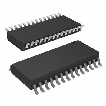
- 封装:28-SOIC(0.295",7.50mm 宽)
- RoHS:无铅 / 符合限制有害物质指令(RoHS)规范要求
- 包装方式:管件
- 参考价格:$11.7-$9.945
更新日期:2024-04-01 00:04:00
产品简介:具有八通道总线收发器和寄存器的扫描测试设备
查看详情- 封装:28-SOIC(0.295",7.50mm 宽)
- RoHS:无铅 / 符合限制有害物质指令(RoHS)规范要求
- 包装方式:管件
- 参考价格:$11.7-$9.945
SN74ABT8652DW 供应商
- 公司
- 型号
- 品牌
- 封装/批号
- 数量
- 地区
- 日期
- 说明
- 询价
-
TI
-
原厂原装
22+ -
3288
-
上海市
-
-
-
一级代理原装
-
TI(德州仪器)
-
SOIC-28
2022+ -
12000
-
上海市
-
-
-
原装可开发票
SN74ABT8652DW 中文资料属性参数
- 标准包装:20
- 类别:集成电路 (IC)
- 家庭:逻辑 - 专用逻辑
- 系列:74ABT
- 逻辑类型:扫描测试设备,带总线收发器和寄存器
- 电源电压:4.5 V ~ 5.5 V
- 位数:8
- 工作温度:-40°C ~ 85°C
- 安装类型:表面贴装
- 封装/外壳:28-SOIC(0.295",7.50mm 宽)
- 供应商设备封装:28-SOIC
- 包装:管件
- 其它名称:296-33634-5SN74ABT8652DW-ND
产品特性
- Members of the Texas Instruments SCOPETM Family of Testability Products
- Compatible With the IEEE Standard 1149.1-1990 (JTAG) Test Access Port and Boundary-Scan Architecture
- Functionally Equivalent to 'F652 and 'ABT652 in the Normal-Function Mode
- SCOPETM Instruction Set IEEE Standard 1149.1-1990 Required Instructions, Optional INTEST, CLAMP, and HIGHZ Parallel-Signature Analysis at Inputs With Masking Option Pseudo-Random Pattern Generation From Outputs Sample Inputs/Toggle Outputs Binary Count From Outputs Even-Parity Opcodes
- IEEE Standard 1149.1-1990 Required Instructions, Optional INTEST, CLAMP, and HIGHZ
- Parallel-Signature Analysis at Inputs With Masking Option
- Pseudo-Random Pattern Generation From Outputs
- Sample Inputs/Toggle Outputs
- Binary Count From Outputs
- Even-Parity Opcodes
- Two Boundary-Scan Cells Per I/O for Greater Flexibility
- State-of-the-Art EPIC-IIBTM BiCMOS Design Significantly Reduces Power Dissipation
- Package Options Include Shrink Small-Outline (DL) and Plastic Small-Outline (DW) Packages, Ceramic Chip Carriers (FK), and Standard Ceramic DIPs (JT)
产品概述
The 'ABT8652 scan test devices with octal bus transceivers and
registers are members of the Texas Instruments SCOPETM
testability integrated-circuit family. This family of devices
supports IEEE Standard 1149.1-1990 boundary scan to facilitate
testing of complex circuit-board assemblies. Scan access to the test
circuitry is accomplished via the 4-wire test access port (TAP)
interface.In the normal mode, these devices are functionally equivalent to
the 'F652 and 'ABT652 octal bus transceivers and registers. The test
circuitry can be activated by the TAP to take snapshot samples of the
data appearing at the device pins or to perform a self test on the
boundary-test cells. Activating the TAP in normal mode does not
affect the functional operation of the SCOPETM octal bus
transceivers and registers. Data flow in each direction is controlled by clock (CLKAB and
CLKBA), select (SAB and SBA), and output-enable (OEAB and ) inputs. For A-to-B data flow,
data on the A bus is clocked into the associated registers on the
low-to-high transition of CLKAB. When SAB is low, real-time A data is
selected for presentation to the B bus (transparent mode). When SAB
is high, stored A data is selected for presentation to the B bus
(registered mode). When OEAB is high, the B outputs are active. When
OEAB is low, the B outputs are in the high-impedance state. Control
for B-to-A data flow is similar to that for A-to-B data flow but uses
CLKBA, SBA, and inputs. Since
the input is
active low, the A outputs are active when is low and are in the
high-impedance state when is
high. Figure 1 shows the four fundamental bus-management functions
that can be performed with the 'ABT8652.In the test mode, the normal operation of the SCOPETM
bus transceivers and registers is inhibited and the test circuitry is
enabled to observe and control the I/O boundary of the device. When
enabled, the test circuitry performs boundary-scan test operations as
described in IEEE Standard 1149.1-1990.Four dedicated test pins control the operation of the test
circuitry: test data input (TDI), test data output (TDO), test mode
select (TMS), and test clock (TCK). Additionally, the test circuitry
performs other testing functions such as parallel-signature analysis
(PSA) on data inputs and pseudo-random pattern generation (PRPG) from
data outputs. All testing and scan operations are synchronized to the
TAP interface.The SN54ABT8652 is characterized for operation over the full
military temperature range of -55°C to 125°C. The
SN74ABT8652 is characterized for operation from -40°C to
85°C.
SN74ABT8652DW 数据手册
| 数据手册 | 说明 | 数量 | 操作 |
|---|---|---|---|
 SN74ABT8652DW SN74ABT8652DW
|
Scan Test Device with Bus Transceiver and Registers IC 28-SOIC |
31页,516K | 查看 |
SN74ABT8652DW 相关产品
- 74ACT1284MTCX
- 74LVC1GX04DCKTG4
- 74LVC1GX04GW,125
- 74SSTUB32868AZRHR
- 74SSTUB32868ZRHR
- 8V182512IDGGREP
- CD4007UBE
- CD4007UBEE4
- CD4007UBM96
- CD4007UBNSR
- CD4007UBPWR
- CD40117BE
- CD4089BE
- CD4089BEE4
- CD4089BNSR
- CD4089BPWR
- CD4527BE
- CD4527BNSR
- CD4527BPWR
- CD74AC283E
- CD74AC283M96
- CD74ACT283E
- CD74ACT283M
- CD74HC283E
- CD74HC283M
- CD74HC283M96
- CD74HCT283E
- CD74HCT283M96
- CLVC1GX04MDRLREP
- MC100E116FNR2G