 搜索
搜索
 发布采购
发布采购
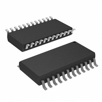
- 封装:24-SOIC(0.295",7.50mm 宽)
- RoHS:无铅 / 符合限制有害物质指令(RoHS)规范要求
- 包装方式:管件
- 参考价格:$1.24-$2.8
更新日期:2024-04-01 00:04:00
产品简介:具有奇偶校验发生器/校验器和三态输出的八路收发器
查看详情- 封装:24-SOIC(0.295",7.50mm 宽)
- RoHS:无铅 / 符合限制有害物质指令(RoHS)规范要求
- 包装方式:管件
- 参考价格:$1.24-$2.8
SN74ABT657ADW 供应商
- 公司
- 型号
- 品牌
- 封装/批号
- 数量
- 地区
- 日期
- 说明
- 询价
-
TI
-
原厂原装
22+ -
3288
-
上海市
-
-
-
一级代理原装
SN74ABT657ADW 中文资料属性参数
- 标准包装:25
- 类别:集成电路 (IC)
- 家庭:逻辑 - 缓冲器,驱动器,接收器,收发器
- 系列:74ABT
- 逻辑类型:收发器,非反相
- 元件数:1
- 每个元件的位元数:8
- 输出电流高,低:32mA,64mA
- 电源电压:4.5 V ~ 5.5 V
- 工作温度:-40°C ~ 85°C
- 安装类型:表面贴装
- 封装/外壳:24-SOIC(0.295",7.50mm 宽)
- 供应商设备封装:24-SOIC
- 包装:管件
- 其它名称:296-4068-5
产品特性
- State-of-the-Art EPIC-II BTM BiCMOS Design Significantly Reduces Power Dissipation
- ESD Protection Exceeds 2000 V Per MIL-STD-883, Method 3015; Exceeds 200 V Using Machine Model (C = 200 pF, R = 0)
- Latch-Up Performance Exceeds 500 mA Per JEDEC Standard JESD-17
- Typical VOLP (Output Ground Bounce) < 1 V at VCC = 5 V, TA = 25°C
- High-Impedance State During Power Up and Power Down
- Flow-Through Architecture Optimizes PCB Layout
- High-Drive Outputs (-32-mA IOH, 64-mA IOL)
- Package Options Include Plastic Small-Outline (DW) Packages, Ceramic Chip Carriers (FK), and Plastic (NT) and Ceramic (JT) DIPs
产品概述
The 'ABT657A transceivers have eight noninverting buffers with parity-generator/
checker circuits and control signals. The transmit/receive (T/R\) input determines the direction of data flow. When T/R\ is high, data flows from the A port to the B port (transmit mode); when T/R\ is low, data flows from the B port to the A port (receive mode). When the output-enable (OE\) input is high, both the A and B ports are in the high-impedance state.
Odd or even parity is selected by a logic high or low level on the ODD/EVEN\ input. PARITY carries the parity-bit value; it is an output from the parity generator/checker in the transmit mode and an input to the parity generator/checker in the receive mode.
In the transmit mode, after the A bus is polled to determine the number of high bits, PARITY is set to the logic level that maintains the parity sense selected by the level at ODD/EVEN\. For example, if ODD/EVEN\ is low (even parity selected) and there are five high bits on the A bus, PARITY is set to the logic high level so that an even number of the nine total bits (eight A-bus bits plus parity bit) are high.
In the receive mode, after the B bus is polled to determine the number of high bits, the error (ERR\) output logic level indicates whether or not the data to be received exhibits the correct parity sense. For example, if ODD/EVEN\ is high (odd parity selected), PARITY is high, and there are three high bits on the B bus, ERR\ is low, indicating a parity error.
When VCC is between 0 and 2.1 V, the device is in the high-impedance state during power up or power down. However, to ensure the high-impedance state above 2.1 V, OE\ should be tied to VCC through a pullup resistor; the minimum value of the resistor is determined by the current-sinking capability of the driver.
The SN54ABT657A is characterized for operation over the full military temperature range of -55°C to 125°C. The SN74ABT657A is characterized for operation from -40°C to 85°C.
SN74ABT657ADW 数据手册
| 数据手册 | 说明 | 数量 | 操作 |
|---|---|---|---|
 SN74ABT657ADW SN74ABT657ADW
|
OCTAL TRANSCEIVERS WITH PARITY GENERATORS/CHECKERS AND 3-STATE OUTPUTS |
9 Pages页,160K | 查看 |
|
SN74ABT657ADW
|
Transceiver, Non-Inverting 1 Element 8 Bit per Element Push-Pull Output 24-SOIC |
13页,354K | 查看 |
|
SN74ABT657ADWR
|
Transceiver, Non-Inverting 1 Element 8 Bit per Element Push-Pull Output 24-SOIC |
13页,354K | 查看 |
SN74ABT657ADW 相关产品
- 100314QC
- 1P1G125QDCKRG4Q1
- 1P1G125QDCKRQ1
- 1P1G126QDBVRQ1
- 74ABT125PW,118
- 74ABT162244CSSX
- 74ABT162244DGGRG4
- 74ABT162245DLRG4
- 74ABT16245ADGGRG4
- 74ABT244D,623
- 74ABT245PW,118
- 74AC11244DBR
- 74AC11244DWR
- 74AC11244PWR
- 74AC11245DW
- 74AC11245DWR
- 74AC16244DGGR
- 74AC16244DL
- 74AC16244DLR
- 74AC16245DLR
- 74AC16652DL
- 74ACT11244DBR
- 74ACT11244DWR
- 74ACT11244PWR
- 74ACT11245DBR
- 74ACT11245DWR
- 74ACT11245NSR
- 74ACT11245PWR
- 74ACT16244DGGR
- 74ACT16244DLR