 搜索
搜索
 发布采购
发布采购
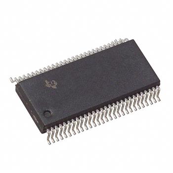
- 封装:56-BSSOP(0.295",7.50mm 宽)
- RoHS:无铅 / 符合限制有害物质指令(RoHS)规范要求
- 包装方式:Digi-Reel®
- 参考价格:$10.0224-$9.0725
更新日期:2024-04-01 00:04:00
产品简介:具有 18 位总线收发器的扫描测试设备
查看详情- 封装:56-BSSOP(0.295",7.50mm 宽)
- RoHS:无铅 / 符合限制有害物质指令(RoHS)规范要求
- 包装方式:Digi-Reel®
- 参考价格:$10.0224-$9.0725
SN74ABT18245ADLR 供应商
- 公司
- 型号
- 品牌
- 封装/批号
- 数量
- 地区
- 日期
- 说明
- 询价
-
TI
-
原厂原装
22+ -
3288
-
上海市
-
-
-
一级代理原装
-
TI
-
标准封装
23+ -
15000
-
上海市
-
-
-
中国区代理原装进口特价
SN74ABT18245ADLR 中文资料属性参数
- 标准包装:1
- 类别:集成电路 (IC)
- 家庭:逻辑 - 专用逻辑
- 系列:74ABT
- 逻辑类型:扫描测试设备,带总线收发器
- 电源电压:4.5 V ~ 5.5 V
- 位数:18
- 工作温度:-40°C ~ 85°C
- 安装类型:表面贴装
- 封装/外壳:56-BSSOP(0.295",7.50mm 宽)
- 供应商设备封装:56-SSOP
- 包装:®
- 其它名称:296-3938-6
产品特性
- Members of the Texas Instruments SCOPETM Family of Testability Products
- Members of the Texas Instruments WidebusTM Family
- Compatible With the IEEE Standard 1149.1-1990 (JTAG) Test Access Port and Boundary-Scan Architecture
- SCOPETM Instruction Set IEEE Standard 1149.1-1990 Required Instructions, CLAMP and HIGHZ Parallel-Signature Analysis at Inputs Pseudo-Random Pattern Generation From Outputs Sample Inputs/Toggle Outputs Binary Count From Outputs Device Identification Even-Parity Opcodes
- IEEE Standard 1149.1-1990 Required Instructions, CLAMP and HIGHZ
- Parallel-Signature Analysis at Inputs
- Pseudo-Random Pattern Generation From Outputs
- Sample Inputs/Toggle Outputs
- Binary Count From Outputs
- Device Identification
- Even-Parity Opcodes
- State-of-the-Art EPIC-II BTM BiCMOS Design Significantly Reduces Power Dissipation
- Packaged in Plastic Shrink Small-Outline (DL) and Thin Shrink Small-Outline (DGG) Packages and 380-mil Fine-Pitch Ceramic Flat (WD) Packages
产品概述
The 'ABT18245A scan test devices with 18-bit bus transceivers are members of the Texas Instruments SCOPETM testability integrated-
circuit family. This family of devices supports IEEE Standard 1149.1-1990 boundary scan to facilitate testing of complex circuit-board assemblies. Scan access to the test circuitry is accomplished via the 4-wire test access port (TAP) interface.
In the normal mode, these devices are 18-bit noninverting bus transceivers. They can be used either as two 9-bit transceivers or one 18-bit transceiver. The test circuitry can be activated by the TAP to take snapshot samples of the data appearing at the device pins or to perform a self-test on the boundary-test cells. Activating the TAP in the normal mode does not affect the functional operation of the SCOPETM bus transceivers.
Data flow is controlled by the direction-control (DIR) and output-enable (OE\) inputs. Data transmission is allowed from the A bus to the B bus or from the B bus to the A bus, depending on the logic level at DIR. OE\ can be used to disable the device so that the buses are effectively isolated.
In the test mode, the normal operation of the SCOPETM bus transceivers is inhibited and the test circuitry is enabled to observe and control the input/output (I/O) boundary of the device. When enabled, the test circuitry performs boundary-scan test operations according to the protocol described in IEEE Standard 1149.1-1990.
Four dedicated test pins observe and control the operation of the test circuitry: test-data input (TDI), test-data output (TDO), test-mode select (TMS), and test clock (TCK). Additionally, the test circuitry performs other testing functions such as parallel-signature analysis (PSA) on data inputs and pseudo-random pattern generation (PRPG) from data outputs. All testing and scan operations are synchronized to the TAP interface.
The SN54ABT18245A is characterized for operation over the full military temperature range of -55°C to 125°C. The SN74ABT18245A is characterized for operation from -40°C to 85°C.
SN74ABT18245ADLR 数据手册
| 数据手册 | 说明 | 数量 | 操作 |
|---|---|---|---|
 SN74ABT18245ADLR SN74ABT18245ADLR
|
Scan Test Device with Bus Transceivers IC 56-SSOP |
37页,1.27M | 查看 |
SN74ABT18245ADLR 相关产品
- 74ACT1284MTCX
- 74LVC1GX04DCKTG4
- 74LVC1GX04GW,125
- 74SSTUB32868AZRHR
- 74SSTUB32868ZRHR
- 8V182512IDGGREP
- CD4007UBE
- CD4007UBEE4
- CD4007UBM96
- CD4007UBNSR
- CD4007UBPWR
- CD40117BE
- CD4089BE
- CD4089BEE4
- CD4089BNSR
- CD4089BPWR
- CD4527BE
- CD4527BNSR
- CD4527BPWR
- CD74AC283E
- CD74AC283M96
- CD74ACT283E
- CD74ACT283M
- CD74HC283E
- CD74HC283M
- CD74HC283M96
- CD74HCT283E
- CD74HCT283M96
- CLVC1GX04MDRLREP
- MC100E116FNR2G