 搜索
搜索
 发布采购
发布采购
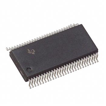
- 封装:56-BSSOP(0.295",7.50mm 宽)
- RoHS:无铅 / 符合限制有害物质指令(RoHS)规范要求
- 包装方式:管件
- 参考价格:$1.75
更新日期:2024-04-01 00:04:00
产品简介:具有三态输出的 16 位总线收发器和寄存器
查看详情- 封装:56-BSSOP(0.295",7.50mm 宽)
- RoHS:无铅 / 符合限制有害物质指令(RoHS)规范要求
- 包装方式:管件
- 参考价格:$1.75
SN74ABT16646DL 供应商
- 公司
- 型号
- 品牌
- 封装/批号
- 数量
- 地区
- 日期
- 说明
- 询价
-
TI
-
原厂原装
22+ -
3288
-
上海市
-
-
-
一级代理原装
-
TI(德州仪器)
-
SSOP-56
2022+ -
12000
-
上海市
-
-
-
原装可开发票
-
TI
-
SSOP
23+ -
15000
-
上海市
-
-
-
中国区代理原装进口特价
SN74ABT16646DL 中文资料属性参数
- 标准包装:20
- 类别:集成电路 (IC)
- 家庭:逻辑 - 缓冲器,驱动器,接收器,收发器
- 系列:74ABT
- 逻辑类型:寄存收发器,非反相
- 元件数:2
- 每个元件的位元数:8
- 输出电流高,低:32mA,64mA
- 电源电压:4.5 V ~ 5.5 V
- 工作温度:-40°C ~ 85°C
- 安装类型:表面贴装
- 封装/外壳:56-BSSOP(0.295",7.50mm 宽)
- 供应商设备封装:56-SSOP
- 包装:管件
产品特性
- Members of the Texas Instruments WidebusTM Family
- State-of-the-Art EPIC-II BTM BiCMOS Design Significantly Reduces Power Dissipation
- Latch-Up Performance Exceeds 500 mA Per JESD 17
- Typical VOLP (Output Ground Bounce) < 1 V at VCC = 5 V, TA = 25°C
- Distributed VCC and GND Pin Configuration Minimizes High-Speed Switching Noise
- Flow-Through Architecture Optimizes PCB Layout
- High-Drive Outputs (-32-mA IOH, 64-mA IOL)
- Package Options Include Plastic Shrink Small-Outline (DL), Thin Shrink Small-Outline (DGG) Packages and 380-mil Fine-Pitch Ceramic Flat (WD) Package Using 25-mil Center-to-Center Spacings
产品概述
The 'ABT16646 devices consist of bus-transceiver circuits, D-type flip-flops, and control circuitry arranged for multiplexed transmission of data directly from the input bus or from the internal registers.
These devices can be used as two 8-bit transceivers or one 16-bit transceiver. Data on the A or B bus is clocked into the registers on the low-to-high transition of the appropriate clock (CLKAB or CLKBA) input. Figure 1 illustrates the four fundamental bus-management functions that can be performed with the 'ABT16646 devices.
Output-enable (OE\) and direction-control (DIR) inputs are provided to control the transceiver functions. In the transceiver mode, data present at the high-impedance port may be stored in either register or in both. The select-control (SAB and SBA) inputs can multiplex stored and real-time (transparent mode) data. The circuitry used for select control eliminates the typical decoding glitch that occurs in a multiplexer during the transition between stored and real-time data. The direction control (DIR) determines which bus receives data when OE\ is low. In the isolation mode (OE\ high), A data can be stored in one register and/or B data can be stored in the other register.
When an output function is disabled, the input function is still enabled and can be used to store and transmit data. Only one of the two buses, A or B, can be driven at a time.
To ensure the high-impedance state during power up or power down, OE\ should be tied to VCC through a pullup resistor; the minimum value of the resistor is determined by the current-sinking capability of the driver.
The SN54ABT16646 is characterized for operation over the full military temperature range of -55°C to 125°C. The SN74ABT16646 is characterized for operation from -40°C to 85°C.
SN74ABT16646DL 数据手册
| 数据手册 | 说明 | 数量 | 操作 |
|---|---|---|---|
 SN74ABT16646DL SN74ABT16646DL
|
16-BIT BUS TRANSCEIVERS AND REGISTERS WITH 3-STATE OUTPUTS |
15 Pages页,248K | 查看 |
|
SN74ABT16646DLR
|
16-BIT BUS TRANSCEIVERS AND REGISTERS WITH 3-STATE OUTPUTS |
15 Pages页,248K | 查看 |
|
SN74ABT16646DLRG4
|
16-BIT BUS TRANSCEIVERS AND REGISTERS WITH 3-STATE OUTPUTS |
15 Pages页,248K | 查看 |
SN74ABT16646DL 相关产品
- 100314QC
- 1P1G125QDCKRG4Q1
- 1P1G125QDCKRQ1
- 1P1G126QDBVRQ1
- 74ABT125PW,118
- 74ABT162244CSSX
- 74ABT162244DGGRG4
- 74ABT162245DLRG4
- 74ABT16245ADGGRG4
- 74ABT244D,623
- 74ABT245PW,118
- 74AC11244DBR
- 74AC11244DWR
- 74AC11244PWR
- 74AC11245DW
- 74AC11245DWR
- 74AC16244DGGR
- 74AC16244DL
- 74AC16244DLR
- 74AC16245DLR
- 74AC16652DL
- 74ACT11244DBR
- 74ACT11244DWR
- 74ACT11244PWR
- 74ACT11245DBR
- 74ACT11245DWR
- 74ACT11245NSR
- 74ACT11245PWR
- 74ACT16244DGGR
- 74ACT16244DLR