
 搜索
搜索
 发布采购
发布采购
更新日期:2024-04-01 00:04:00

产品简介:汽车类 5.5V 至 65V 高侧保护控制器
查看详情LM5060QDGSRQ1 供应商
- 公司
- 型号
- 品牌
- 封装/批号
- 数量
- 地区
- 日期
- 说明
- 询价
-
TI
-
原厂原装
22+ -
3288
-
上海市
-
-
-
一级代理原装
LM5060QDGSRQ1 中文资料属性参数
- 现有数量:0现货查看交期
- 价格:1 : ¥18.92000剪切带(CT)3,500 : ¥9.62336卷带(TR)
- 系列:Automotive, AEC-Q100
- 包装:卷带(TR)剪切带(CT)Digi-Reel? 得捷定制卷带
- 产品状态:在售
- Digi-Key Programmable:Not Verified
- 驱动配置:高端
- 通道类型:单路
- 驱动器数:1
- 栅极类型:N 沟道 MOSFET
- 电压 - 供电:5.5V ~ 65V
- 逻辑电压?- VIL,VIH:0.8V,2V
- 电流 - 峰值输出(灌入,拉出):24μA,2.2mA
- 输入类型:非反相
- 高压侧电压 - 最大值(自举):-
- 上升/下降时间(典型值):-
- 工作温度:-40°C ~ 125°C(TJ)
- 安装类型:表面贴装型
- 封装/外壳:10-TFSOP,10-MSOP(0.118",3.00mm 宽)
- 供应商器件封装:10-VSSOP
产品特性
- Available in Automotive Grade / AEC Q-100
- Wide operating input voltage range: 5.5 V to 65 V
- Functional safety capable Documentation available to aid functional safety system design
- Documentation available to aid functional safety system design
- Less than 15-µA quiescent current in disabled mode
- Controlled output rise time for safe connection of capacitive loads
- Charge pump gate driver for external N-Channel MOSFET
- Adjustable Undervoltage Lockout (UVLO) with hysteresis
- UVLO Serves as second enable input for systems requiring safety redundancy
- Programmable fault detection delay time
- MOSFET latched off after load fault is detected
- Active low open drain POWER GOOD (nPGD) output
- Adjustable input Overvoltage Protection (OVP)
- Immediate restart after overvoltage shutdown
- 10-Lead VSSOP
产品概述
The LM5060 high-side protection controller provides intelligent control of a high-side
N-channel MOSFET during normal on/off transitions and fault conditions. In-rush current is
controlled by the nearly constant rise time of the output voltage. A POWER GOOD output indicates
when the output voltage reaches the input voltage and the MOSFET is fully on. Input UVLO (with
hysteresis) is provided as well as programmable input OVP. An enable input provides remote on or
off control. The programmable UVLO input can be used as second enable input for safety redundancy.
A single capacitor programs the initial start-up VGS fault detection delay
time, the transition VDS fault detection delay time, and the continuous
over-current VDS fault detection delay time. When a detected fault condition
persists longer than the allowed fault delay time, the MOSFET is latched off until either the
enable input or the UVLO input is toggled low and then high.
LM5060QDGSRQ1 电路图
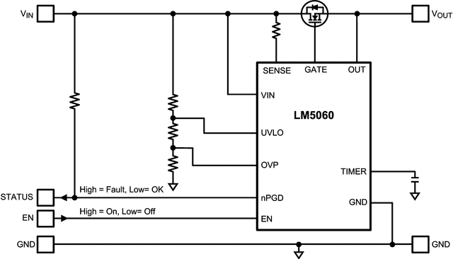
LM5060QDGSRQ1 电路图
LM5060QDGSRQ1 相关产品
- 2SD300C17A1
- 2SP0115T2A0-12
- 5962-1022101VSC
- 5962-8686102XA
- 5962-8688202XA
- 5962-89728022A
- 5962-89805012A
- 5962-8982402PA
- 5962-9322201MEA
- 7604501EA
- 85514012A
- 8551401PA
- 905X0205100
- 90E23PYGI8
- 90E24PYGI8
- 90E36ERGI
- A4910KJPTR-T
- A4915METTR-T
- A4930GETTR-T
- A4990KLPTR-T
- A5974AD
- A5974D
- A5975D
- A8304SESTR-T
- AAT2153IVN-0.6-T1
- AAT2823IBK-1-T1
- AAT4684ITP-T1
- AD536ASD/883B
- AD536ASH/883B
- AD580SH/883B