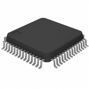
- 封装:56-TFSOP(0.240",6.10mm 宽)
- RoHS:无铅 / 符合限制有害物质指令(RoHS)规范要求
- 包装方式:Digi-Reel®
- 参考价格:$1.8-$3.6
更新日期:2024-04-01 00:04:00
产品简介:具有三态输出的增强型产品 3.3V ABT 16 位寄存收发器
查看详情- 封装:56-TFSOP(0.240",6.10mm 宽)
- RoHS:无铅 / 符合限制有害物质指令(RoHS)规范要求
- 包装方式:Digi-Reel®
- 参考价格:$1.8-$3.6
CLVTH16543IDGGREP 供应商
- 公司
- 型号
- 品牌
- 封装/批号
- 数量
- 地区
- 日期
- 说明
- 询价
-
TI
-
原厂原装
22+ -
3288
-
上海市
-
-
-
一级代理原装
CLVTH16543IDGGREP 中文资料属性参数
- 标准包装:1
- 类别:集成电路 (IC)
- 家庭:逻辑 - 缓冲器,驱动器,接收器,收发器
- 系列:74LVTH
- 逻辑类型:寄存收发器,非反相
- 元件数:2
- 每个元件的位元数:8
- 输出电流高,低:32mA,64mA
- 电源电压:2.7 V ~ 3.6 V
- 工作温度:-40°C ~ 85°C
- 安装类型:表面贴装
- 封装/外壳:56-TFSOP(0.240",6.10mm 宽)
- 供应商设备封装:56-TSSOP
- 包装:®
- 其它名称:296-22139-6
产品特性
- Controlled Baseline One Assembly/Test Site, One Fabrication Site
- One Assembly/Test Site, One Fabrication Site
- Enhanced Diminishing Manufacturing Sources (DMS) Support
- Enhanced Product–Change Notification
- Qualification Pedigree(1)
- Member of the Texas Instruments Widebus™ Family
- State–of–the–Art Advanced BiCMOS Technology (ABT) Design for 3.3–V Operation and Low Static–Power Dissipation
- Supports Mixed–Mode Signal Operation (5–V Input and Output Voltages With 3.3–V VCC)
- Supports Unregulated Battery Operation Down to 2.7 V
- Ioff and Power–Up 3–State Support Hot Insertion
- Bus Hold on Data Inputs Eliminates the Need for External Pullup/Pulldown Resistors
- Typical VOLP (Output Ground Bounce)<0.8 V at VCC = 3.3 V, TA = 25°C
- Distributed VCC and GND Pins Minimize High–Speed Switching Noise
- Flow–Through Architecture Optimizes PCB Layout
- Latch–Up Performance Exceeds 500 mA Per JESD 17
- ESD Protection Exceeds 2000 V Per MIL–STD–883, Method 3015; Exceeds 200 V Using Machine Model (C = 200 pF, R = 0)
产品概述
The SN74LVTH16543 is a 16–bit registered transceiver designed for low–voltage (3.3–V) VCC operation, but with the capability to provide a TTL interface to a 5–V system environment. This device can be used as two 8–bit transceivers or one 16–bit transceiver. Separate latch–enable (LEAB or LEBA) and output–enable (OEAB or OEBA) inputs are provided for each register to permit independent control in either direction of data flow.The A–to–B enable (CEAB) input must be low to enter data from A or to output data from B. If CEAB is low and LEAB is low, the A–to–B latches are transparent; a subsequent low–to–high transition of LEAB puts the A latches in the storage mode. With CEAB and OEAB both low, the 3–state B outputs are active and reflect the data present at the output of the A latches. Data flow from B to A is similar, but requires using the CEBA, LEBA, and OEBA inputs.Active bus–hold circuitry is provided to hold unused or floating data inputs at a valid logic level.When VCC is between 0 and 1.5 V, the device is in the high–impedance state during power up or power down. However, to ensure the high–impedance state above 1.5 V, OE should be tied to VCC through a pullup resistor; the minimum value of the resistor is determined by the current–sinking capability of the driver.This device is fully specified for hot–insertion applications using Ioff and power–up 3–state. The Ioff circuitry disables the outputs, preventing damaging current backflow through the device when it is powered down. The power–up 3–state circuitry places the outputs in the high–impedance state during power up and power down, which prevents driver conflict.
CLVTH16543IDGGREP 数据手册
| 数据手册 | 说明 | 数量 | 操作 |
|---|---|---|---|
 CLVTH16543IDGGREP CLVTH16543IDGGREP
|
Transceiver, Non-Inverting 2 Element 8 Bit per Element Push-Pull Output 56-TSSOP |
12页,299K | 查看 |
CLVTH16543IDGGREP 相关产品
- 100314QC
- 1P1G125QDCKRG4Q1
- 1P1G125QDCKRQ1
- 1P1G126QDBVRQ1
- 74ABT125PW,118
- 74ABT162244CSSX
- 74ABT162244DGGRG4
- 74ABT162245DLRG4
- 74ABT16245ADGGRG4
- 74ABT244D,623
- 74ABT245PW,118
- 74AC11244DBR
- 74AC11244DWR
- 74AC11244PWR
- 74AC11245DW
- 74AC11245DWR
- 74AC16244DGGR
- 74AC16244DL
- 74AC16244DLR
- 74AC16245DLR
- 74AC16652DL
- 74ACT11244DBR
- 74ACT11244DWR
- 74ACT11244PWR
- 74ACT11245DBR
- 74ACT11245DWR
- 74ACT11245NSR
- 74ACT11245PWR
- 74ACT16244DGGR
- 74ACT16244DLR

 搜索
搜索
 发布采购
发布采购
