 搜索
搜索
 发布采购
发布采购
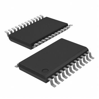
- 封装:24-TSSOP(0.173",4.40mm 宽)
- RoHS:无铅 / 符合限制有害物质指令(RoHS)规范要求
- 包装方式:管件
- 参考价格:$3.038-$6.86
更新日期:2024-04-01 00:04:00
产品简介:适用于通用应用且支持高达 105°C 温度的高性能 1:10 时钟缓冲器
查看详情- 封装:24-TSSOP(0.173",4.40mm 宽)
- RoHS:无铅 / 符合限制有害物质指令(RoHS)规范要求
- 包装方式:管件
- 参考价格:$3.038-$6.86
CDCVF2310PW 供应商
- 公司
- 型号
- 品牌
- 封装/批号
- 数量
- 地区
- 日期
- 说明
- 询价
-
TI
-
原厂原装
22+ -
3288
-
上海市
-
-
-
一级代理原装
-
-
2019+ -
5800
-
上海市
-
-
-
全新原装现货
-
TI(德州仪器)
-
TSSOP-24
2022+ -
12000
-
上海市
-
-
-
原装可开发票
-
TI
-
TSSOP24
23+ -
15000
-
上海市
-
-
-
中国区代理原装现货热卖特价
-
TI
-
TSSOP
23+ -
46000
-
合肥
-
-
-
科大讯飞战略投资企业,提供一站式配套服务
-
TI
-
TSSOP-24
23+ -
5800
-
上海市
-
-
-
进口原装现货,杜绝假货。
-
TI
-
-
15+ -
2000
-
杭州
-
-
-
原装正品
-
TI/德州仪器
-
TSSOP24
21+ -
2000
-
杭州
-
-
-
只做原装现货,大量现货热卖
-
TI
-
-
21+ -
12500
-
上海市
-
-
-
原装现货,品质为先!请来电垂询!
CDCVF2310PW 中文资料属性参数
- 标准包装:60
- 类别:集成电路 (IC)
- 家庭:时钟/计时 - 时钟缓冲器,驱动器
- 系列:-
- 类型:扇出缓冲器(分配)
- 电路数:1
- 比率 - 输入:输出:1:10
- 差分 - 输入:输出:无/无
- 输入:LVTTL
- 输出:LVTTL
- 频率 - 最大:200MHz
- 电源电压:2.3 V ~ 3.6 V
- 工作温度:-40°C ~ 85°C
- 安装类型:表面贴装
- 封装/外壳:24-TSSOP(0.173",4.40mm 宽)
- 供应商设备封装:24-TSSOP
- 包装:管件
- 其它名称:296-12019-5
产品特性
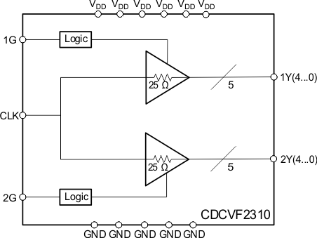
- High-Performance 1:10 Clock Driver
- Operates up to 200 MHz at VDD 3.3 V
- Pin-to-Pin Skew < 100 ps at VDD 3.3 V
- VDD Range: 2.3 V to 3.6 V
- Operating Temperature Range –40°C to 105°C
- Supports 105ºC Ambient Temperature (see Thermal Considerations)
- Output Enable Glitch Suppression
- Distributes One Clock Input to Two Banks of Five Outputs
- 25-Ω On-Chip Series Damping Resistors
- Packaged in 24-Pin TSSOP
产品概述
The CDCVF2310 device is a high-performance, low-skew clock buffer that operates up to 200
MHz. Two banks of five outputs each provide low-skew copies of CLK. After power up, the default
state of the outputs is low regardless of the state of the control pins. For normal operation, the
outputs of bank 1Y[0:4] or 2Y[0:4] can be placed in a low state when the control pins (1G or 2G,
respectively) are held low and a negative clock edge is detected on the CLK input. The outputs of
bank 1Y[0:4] or 2Y[0:4] can be switched into the buffer mode when the control pins (1G and 2G) are
held high and a negative clock edge is detected on the CLK input. The device operates in a 2.5-V
and 3.3-V environment. The built-in output enable glitch suppression ensures a synchronized output
enable sequence to distribute full period clock signals.The CDCVF2310 is characterized for operation from –40°C to 85°C.
CDCVF2310PW 数据手册
| 数据手册 | 说明 | 数量 | 操作 |
|---|---|---|---|
 CDCVF2310PW CDCVF2310PW
|
High Performance 1:10 Clock Buffer for General Purpose Applications 24-TSSOP -40 to 85 |
14页,339K | 查看 |
|
CDCVF2310PW
|
Clock Fanout Buffer (Distribution) IC 200MHz 24-TSSOP (0.173", 4.40mm Width) |
23页,879K | 查看 |
CDCVF2310PW 电路图
CDCVF2310PW 电路图
CDCVF2310PW 相关产品
- ADCLK854BCPZ
- ADCLK907BCPZ-R2
- ADCLK907BCPZ-R7
- ADCLK914BCPZ-R2
- ADCLK914BCPZ-WP
- ADCLK925BCPZ-R7
- ADCLK944BCPZ-R2
- ADCLK944BCPZ-R7
- ADCLK944BCPZ-WP
- ADN4670BCPZ
- ADN4670BCPZ-REEL7
- CDC1104RVKR
- CDC111FN
- CDC204DW
- CDC204DWG4
- CDC208DW
- CDC208DWR
- CDC208NS
- CDC208NSR
- CDC2351DB
- CDC2351DBR
- CDC2351DW
- CDC2351DWR
- CDC2351DWRG4
- CDC2351MDBREP
- CDC2351QDB
- CDC2351QDBG4
- CDC2351QDBR
- CDC2351QDBRG4
- CDC318ADL