 搜索
搜索
 发布采购
发布采购
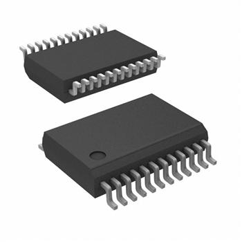
- 封装:24-SSOP(0.209",5.30mm 宽)
- RoHS:无铅 / 符合限制有害物质指令(RoHS)规范要求
- 包装方式:Digi-Reel®
- 参考价格:$12.1245-$20.09
更新日期:2024-04-01 00:04:00
产品简介:具有三态输出的 1 线路至 10 线路时钟驱动器(增强型产品)
查看详情- 封装:24-SSOP(0.209",5.30mm 宽)
- RoHS:无铅 / 符合限制有害物质指令(RoHS)规范要求
- 包装方式:Digi-Reel®
- 参考价格:$12.1245-$20.09
CDC2351MDBREP 供应商
- 公司
- 型号
- 品牌
- 封装/批号
- 数量
- 地区
- 日期
- 说明
- 询价
-
TI
-
原厂原装
22+ -
3288
-
上海市
-
-
-
一级代理原装
-
TI ?
-
SMD
5 -
1500
-
杭州
-
-
-
原装正品现货
-
TI(德州仪器)
-
SSOP-24
2022+ -
12000
-
上海市
-
-
-
原装可开发票
CDC2351MDBREP 中文资料属性参数
- 标准包装:1
- 类别:集成电路 (IC)
- 家庭:时钟/计时 - 时钟缓冲器,驱动器
- 系列:-
- 类型:扇出缓冲器(分配)
- 电路数:1
- 比率 - 输入:输出:1:10
- 差分 - 输入:输出:无/无
- 输入:LVTTL
- 输出:LVTTL
- 频率 - 最大:100MHz
- 电源电压:3 V ~ 3.6 V
- 工作温度:-55°C ~ 125°C
- 安装类型:表面贴装
- 封装/外壳:24-SSOP(0.209",5.30mm 宽)
- 供应商设备封装:24-SSOP
- 包装:®
- 其它名称:296-18093-6
产品特性
- Controlled Baseline One Assembly/Test Site, One Fabrication Site
- One Assembly/Test Site, One Fabrication Site
- Extended Temperature Performance of –55°C to 125°C
- Enhanced Diminishing Manufacturing Sources (DMS) Support
- Enhanced Product-Change Notification
- Qualification Pedigree
- Low Output Skew, Low Pulse Skew for Clock-Distribution and Clock-Generation Applications
- Operates at 3.3-V VCC
- LVTTL-Compatible Inputs and Outputs
- Supports Mixed-Mode Signal Operation (5-V Input and Output Voltages With 3.3-V VCC)
- Distributes One Clock Input to 10 Outputs
- Outputs Have Internal Series Damping Resistor to Reduce Transmission Line Effects
- Distributed VCC and Ground Pins Reduce Switching Noise
- State-of-the-Art EPIC-IIB™ BiCMOS Design Significantly Reduces Power Dissipation
- Shrink Small-Outline (DB) Package
产品概述
The CDC2351 is a high-performance clock-driver circuit that distributes one input (A) to 10 outputs (Y) with minimum skew for clock distribution. The output-enable (OE)\ input disables the outputs to a high-impedance state. Each output has an internal series damping resistor to improve signal integrity at the load. The CDC2351 operates at nominal 3.3-V VCC.The propagation delays are adjusted at the factory using the P0 and P1 pins. The factory adjustments ensure that the part-to-part skew is minimized and is kept within a specified window. Pins P0 and P1 are not intended for customer use and should be connected to GND.The CDC2351M is characterized for operation over the full military temperature range of –55°C to 125°C.
CDC2351MDBREP 数据手册
| 数据手册 | 说明 | 数量 | 操作 |
|---|---|---|---|
 CDC2351MDBREP CDC2351MDBREP
|
Clock Fanout Buffer (Distribution) IC 100MHz 24-SSOP (0.209", 5.30mm Width) |
11页,454K | 查看 |
CDC2351MDBREP 相关产品
- ADCLK854BCPZ
- ADCLK907BCPZ-R2
- ADCLK907BCPZ-R7
- ADCLK914BCPZ-R2
- ADCLK914BCPZ-WP
- ADCLK925BCPZ-R7
- ADCLK944BCPZ-R2
- ADCLK944BCPZ-R7
- ADCLK944BCPZ-WP
- ADN4670BCPZ
- ADN4670BCPZ-REEL7
- CDC1104RVKR
- CDC111FN
- CDC204DW
- CDC204DWG4
- CDC208DW
- CDC208DWR
- CDC208NS
- CDC208NSR
- CDC2351DB
- CDC2351DBR
- CDC2351DW
- CDC2351DWR
- CDC2351DWRG4
- CDC2351QDB
- CDC2351QDBG4
- CDC2351QDBR
- CDC2351QDBRG4
- CDC318ADL
- CDC318ADLG4