 搜索
搜索
 发布采购
发布采购
- 封装:40-VFQFN 裸露焊盘
- RoHS:无铅 / 符合限制有害物质指令(RoHS)规范要求
- 包装方式:Digi-Reel®
- 参考价格:$13.125-$17.03
更新日期:2024-04-01 00:04:00
产品简介:低抖动 2 路输入可选 1:12 通用至 LVPECL 缓冲器
查看详情- 封装:40-VFQFN 裸露焊盘
- RoHS:无铅 / 符合限制有害物质指令(RoHS)规范要求
- 包装方式:Digi-Reel®
- 参考价格:$13.125-$17.03
CDCLVP1212RHAT 供应商
- 公司
- 型号
- 品牌
- 封装/批号
- 数量
- 地区
- 日期
- 说明
- 询价
-
TI
-
原厂原装
22+ -
3288
-
上海市
-
-
-
一级代理原装
-
TI(德州仪器)
-
VQFN-48
2022+ -
12000
-
上海市
-
-
-
原装可开发票
-
TI
-
原厂原封装
新批号 -
887000
-
上海市
-
-
-
原厂发货进口原装微信同步QQ893727827
-
TI
-
TSSOP
23+ -
46000
-
合肥
-
-
-
科大讯飞战略投资企业,提供一站式配套服务
CDCLVP1212RHAT 中文资料属性参数
- 标准包装:1
- 类别:集成电路 (IC)
- 家庭:时钟/计时 - 时钟缓冲器,驱动器
- 系列:-
- 类型:扇出缓冲器(分配),多路复用器
- 电路数:1
- 比率 - 输入:输出:2:12
- 差分 - 输入:输出:是/是
- 输入:LVCMOS,LVDS,LVPECL,LVTTL
- 输出:LVPECL
- 频率 - 最大:2GHz
- 电源电压:2.375 V ~ 3.6 V
- 工作温度:-40°C ~ 85°C
- 安装类型:表面贴装
- 封装/外壳:40-VFQFN 裸露焊盘
- 供应商设备封装:40-VQFN-EP(6x6)
- 包装:®
- 其它名称:296-25141-6
产品特性
- 2:12 Differential Buffer
- Selectable Clock Inputs Through Control Terminal
- Universal Inputs Accept LVPECL, LVDS, and LVCMOS/LVTTL
- 12 LVPECL Outputs
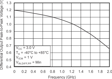
- Maximum Clock Frequency: 2 GHz
- Maximum Core Current Consumption: 88 mA
- Very Low Additive Jitter: <100 fs, rms in 10-kHz to 20-MHz Offset Range: 57 fs, rms (typ) @ 122.88 MHz 48 fs, rms (typ) @ 156.25 MHz 30 fs, rms (typ) @ 312.5 MHz
- 57 fs, rms (typ) @ 122.88 MHz
- 48 fs, rms (typ) @ 156.25 MHz
- 30 fs, rms (typ) @ 312.5 MHz
- 2.375-V to 3.6-V Device Power Supply
- Maximum Propagation Delay: 550 ps
- Maximum Output Skew: 25 ps
- LVPECL Reference Voltage, VAC_REF, Available for Capacitive-Coupled Inputs
- Industrial Temperature Range: –40°C to 85°C
- ESD Protection Exceeds 2 kV (HBM)
- Supports 105°C PCB Temperature (Measured with a Thermal Pad)
- Available in 6-mm × 6-mm QFN-40 (RHA) Package
产品概述
The CDCLVP1212 is a highly versatile, low additive jitter buffer that can generate 12
copies of LVPECL clock outputs from one of two selectable LVPECL, LVDS, or LVCMOS inputs for a
variety of communication applications. It has a maximum clock frequency up to 2 GHz. The CDCLVP1212
features an on-chip multiplexer (MUX) for selecting one of two inputs that can be easily configured
solely through a control terminal. The overall additive jitter performance is less than 0.1 ps, RMS
from 10 kHz to 20 MHz, and overall output skew is as low as 25 ps, making the device a perfect
choice for use in demanding applications.The CDCLVP1212 clock buffer distributes one of two selectable clock inputs (IN0, IN1) to
12 pairs of differential LVPECL clock outputs (OUT0, OUT11) with minimum skew for clock
distribution. The CDCLVP1212 can accept two clock sources into an input multiplexer. The inputs can
be LVPECL, LVDS, or LVCMOS/LVTTL.The CDCLVP1212 is specifically designed for driving 50-Ω transmission lines. When driving
the inputs in single-ended mode, the LVPECL bias voltage (VAC_REF) should be
applied to the unused negative input terminal. However, for high-speed performance up to 2 GHz,
differential mode is strongly recommended. The CDCLVP1212 is packaged in a small 40-terminal, 6-mm × 6-mm QFN package and is
characterized for operation from –40°C to 85°C.
CDCLVP1212RHAT 数据手册
| 数据手册 | 说明 | 数量 | 操作 |
|---|---|---|---|
 CDCLVP1212RHAT CDCLVP1212RHAT
|
Clock Fanout Buffer (Distribution), Multiplexer IC 2GHz 40-VFQFN Exposed Pad |
30页,1.11M | 查看 |
CDCLVP1212RHAT 电路图
CDCLVP1212RHAT 电路图
CDCLVP1212RHAT 相关产品
- ADCLK854BCPZ
- ADCLK907BCPZ-R2
- ADCLK907BCPZ-R7
- ADCLK914BCPZ-R2
- ADCLK914BCPZ-WP
- ADCLK925BCPZ-R7
- ADCLK944BCPZ-R2
- ADCLK944BCPZ-R7
- ADCLK944BCPZ-WP
- ADN4670BCPZ
- ADN4670BCPZ-REEL7
- CDC1104RVKR
- CDC111FN
- CDC204DW
- CDC204DWG4
- CDC208DW
- CDC208DWR
- CDC208NS
- CDC208NSR
- CDC2351DB
- CDC2351DBR
- CDC2351DW
- CDC2351DWR
- CDC2351DWRG4
- CDC2351MDBREP
- CDC2351QDB
- CDC2351QDBG4
- CDC2351QDBR
- CDC2351QDBRG4
- CDC318ADL