 搜索
搜索
 发布采购
发布采购
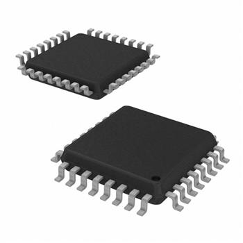
- 封装:32-LQFP
- RoHS:无铅 / 符合限制有害物质指令(RoHS)规范要求
- 包装方式:带卷 (TR)
- 参考价格:$7.382
更新日期:2024-04-01 00:04:00
产品简介:具有可选输入的 1:10 LVPECL 缓冲器
查看详情- 封装:32-LQFP
- RoHS:无铅 / 符合限制有害物质指令(RoHS)规范要求
- 包装方式:带卷 (TR)
- 参考价格:$7.382
CDCLVP111VFR 供应商
- 公司
- 型号
- 品牌
- 封装/批号
- 数量
- 地区
- 日期
- 说明
- 询价
-
TI
-
原厂原装
22+ -
3288
-
上海市
-
-
-
一级代理原装
-
TI/德州仪器
-
LQFP32
21+ -
11611
-
杭州
-
-
-
只做原装现货,大量现货热卖
-
TI(德州仪器)
-
LQFP-32
2022+ -
12000
-
上海市
-
-
-
原装可开发票
-
TI
-
TSSOP
23+ -
46000
-
合肥
-
-
-
科大讯飞战略投资企业,提供一站式配套服务
CDCLVP111VFR 中文资料属性参数
- 标准包装:1,000
- 类别:集成电路 (IC)
- 家庭:时钟/计时 - 时钟缓冲器,驱动器
- 系列:-
- 类型:扇出缓冲器(分配),多路复用器
- 电路数:1
- 比率 - 输入:输出:2:10
- 差分 - 输入:输出:是/是
- 输入:CML,LVDS,LVPECL,SSTL
- 输出:LVPECL
- 频率 - 最大:3.5GHz
- 电源电压:2.375 V ~ 3.8 V
- 工作温度:-40°C ~ 85°C
- 安装类型:表面贴装
- 封装/外壳:32-LQFP
- 供应商设备封装:32-LQFP(7x7)
- 包装:带卷 (TR)
产品特性
- Distributes One Differential Clock Input Pair LVPECL to 10 Differential LVPECL
- Fully Compatible With LVECL and LVPECL
- Supports a Wide Supply Voltage Range from 2.375 V to 3.8 V
- Selectable Clock Input Through CLK_SEL
- Low-Output Skew (Typical 15 ps) for Clock- Distribution Applications Additive Jitter Less Than 1 ps Propagation Delay Less Than 350 ps Open Input Default State LVDS, CML, SSTL Input Compatible
- Additive Jitter Less Than 1 ps
- Propagation Delay Less Than 350 ps
- Open Input Default State
- LVDS, CML, SSTL Input Compatible
- VBB Reference Voltage Output for Single-Ended Clocking
- Available in a 32-Pin LQFP and QFN Package
- Frequency Range From DC to 3.5 GHz
- Pin-to-Pin Compatible With MC100 Series EP111, ES6111, LVEP111, PTN1111
- APPLICATIONS Designed for Driving 50-Ω Transmission Lines High Performance Clock Distribution
- Designed for Driving 50-Ω Transmission Lines
- High Performance Clock Distribution
产品概述
The CDCLVP111 clock driver distributes one differential clock pair of LVPECL input,
(CLK0, CLK1) to ten pairs of differential LVPECL clock (Q0, Q9) outputs with minimum skew for clock
distribution. The CDCLVP111 can accept two clock sources into an input multiplexer. The CDCLVP111
is specifically designed for driving 50-Ω transmission lines. When an output pin is not used,
leaving it open is recommended to reduce power consumption. If only one of the output pins from a
differential pair is used, the other output pin must be identically terminated to 50 Ω.The VBB reference voltage output is used if single-ended input
operation is required. In this case, the VBB pin should be connected to
CLK0 and bypassed to GND through a 10-nF capacitor.However, for high-speed performance up to 3.5 GHz, the differential mode is strongly
recommended.The CDCLVP111 device is characterized for operation from –40°C to 85°C.
CDCLVP111VFR 电路图
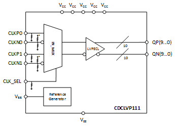
CDCLVP111VFR 电路图
CDCLVP111VFR 相关产品
- ADCLK854BCPZ
- ADCLK907BCPZ-R2
- ADCLK907BCPZ-R7
- ADCLK914BCPZ-R2
- ADCLK914BCPZ-WP
- ADCLK925BCPZ-R7
- ADCLK944BCPZ-R2
- ADCLK944BCPZ-R7
- ADCLK944BCPZ-WP
- ADN4670BCPZ
- ADN4670BCPZ-REEL7
- CDC1104RVKR
- CDC111FN
- CDC204DW
- CDC204DWG4
- CDC208DW
- CDC208DWR
- CDC208NS
- CDC208NSR
- CDC2351DB
- CDC2351DBR
- CDC2351DW
- CDC2351DWR
- CDC2351DWRG4
- CDC2351MDBREP
- CDC2351QDB
- CDC2351QDBG4
- CDC2351QDBR
- CDC2351QDBRG4
- CDC318ADL