 搜索
搜索
 发布采购
发布采购
- 封装:48-VFQFN 裸露焊盘
- RoHS:无铅 / 符合限制有害物质指令(RoHS)规范要求
- 包装方式:带卷 (TR)
- 参考价格:$7.296
更新日期:2024-04-01 00:04:00
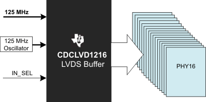
产品简介:低抖动 2 路输入可选 1:16 通用至 LVDS 缓冲器
查看详情- 封装:48-VFQFN 裸露焊盘
- RoHS:无铅 / 符合限制有害物质指令(RoHS)规范要求
- 包装方式:带卷 (TR)
- 参考价格:$7.296
CDCLVD1216RGZR 供应商
- 公司
- 型号
- 品牌
- 封装/批号
- 数量
- 地区
- 日期
- 说明
- 询价
-
TI
-
原厂原装
22+ -
3288
-
上海市
-
-
-
一级代理原装
-
TI(德州仪器)
-
VQFN-48
2022+ -
12000
-
上海市
-
-
-
原装可开发票
-
TI
-
TSSOP
23+ -
46000
-
合肥
-
-
-
科大讯飞战略投资企业,提供一站式配套服务
CDCLVD1216RGZR 中文资料属性参数
- 标准包装:2,500
- 类别:集成电路 (IC)
- 家庭:时钟/计时 - 时钟缓冲器,驱动器
- 系列:-
- 类型:扇出缓冲器(分配),多路复用器
- 电路数:1
- 比率 - 输入:输出:2:16
- 差分 - 输入:输出:是/是
- 输入:LVCMOS,LVDS,LVPECL
- 输出:LVDS
- 频率 - 最大:800MHz
- 电源电压:2.375 V ~ 2.625 V
- 工作温度:-40°C ~ 85°C
- 安装类型:表面贴装
- 封装/外壳:48-VFQFN 裸露焊盘
- 供应商设备封装:48-VQFN 裸露焊盘(7x7)
- 包装:带卷 (TR)
产品特性
- 2:16 Differential Buffer
- Low Additive Jitter: <300 fs RMS in 10 kHz to 20 MHz
- Low Output Skew of 55 ps (Max)
- Universal Inputs Accept LVDS, LVPECL, LVCMOS
- Selectable Clock Inputs Through Control Pin
- 16 LVDS Outputs, ANSI EIA/TIA-644A Standard Compatible
- Clock Frequency up to 800 MHz
- 2.375–2.625V Device Power Supply
- LVDS Reference Voltage, VAC_REF, Available for Capacitive Coupled Inputs
- Industrial Temperature Range –40°C to 85°C
- Packaged in 7mm × 7mm 48-Pin QFN (RGZ)
- ESD Protection Exceeds 3 kV HBM, 1 kV CDM
- APPLICATIONS Telecommunications/Networking Medical Imaging Test and Measurement Equipment Wireless Communications General Purpose Clocking
- Telecommunications/Networking
- Medical Imaging
- Test and Measurement Equipment
- Wireless Communications
- General Purpose Clocking
产品概述
The CDCLVD1216 clock buffer distributes one of two selectable clock inputs (IN0, IN1) to 16 pairs of differential LVDS clock outputs (OUT0, OUT15) with minimum skew for clock distribution. The CDCLVD1216 can accept two clock sources into an input multiplexer. The inputs can either be LVDS, LVPECL, or LVCMOS.The CDCLVD1216 is specifically designed for driving 50 Ω transmission lines. If driving the inputs in single ended mode, the appropriate bias voltage (VAC_REF) should be applied to the unused negative input pin.The IN_SEL pin selects the input which is routed to the outputs. If this pin is left open it disables the outputs (static). The part supports a fail safe function. It incorporates an input hysteresis, which prevents random oscillation of the outputs in absence of an input signal.The device operates in 2.5 V supply environment and is characterized from –40°C to 85°C (ambient temperature). The CDCLVD1216 is packaged in small 48-pin, 7mm × 7mm QFN package.
CDCLVD1216RGZR 电路图
CDCLVD1216RGZR 电路图
CDCLVD1216RGZR 相关产品
- ADCLK854BCPZ
- ADCLK907BCPZ-R2
- ADCLK907BCPZ-R7
- ADCLK914BCPZ-R2
- ADCLK914BCPZ-WP
- ADCLK925BCPZ-R7
- ADCLK944BCPZ-R2
- ADCLK944BCPZ-R7
- ADCLK944BCPZ-WP
- ADN4670BCPZ
- ADN4670BCPZ-REEL7
- CDC1104RVKR
- CDC111FN
- CDC204DW
- CDC204DWG4
- CDC208DW
- CDC208DWR
- CDC208NS
- CDC208NSR
- CDC2351DB
- CDC2351DBR
- CDC2351DW
- CDC2351DWR
- CDC2351DWRG4
- CDC2351MDBREP
- CDC2351QDB
- CDC2351QDBG4
- CDC2351QDBR
- CDC2351QDBRG4
- CDC318ADL