 搜索
搜索
 发布采购
发布采购
- 封装:20-UFBGA,DSBGA
- RoHS:无铅 / 符合限制有害物质指令(RoHS)规范要求
- 包装方式:Digi-Reel®
- 参考价格:$2.592-$5.18
更新日期:2024-04-01 00:04:00

产品简介:具有 LDO 的四通道正弦波时钟缓冲器
查看详情- 封装:20-UFBGA,DSBGA
- RoHS:无铅 / 符合限制有害物质指令(RoHS)规范要求
- 包装方式:Digi-Reel®
- 参考价格:$2.592-$5.18
CDC3S04YFFR 供应商
- 公司
- 型号
- 品牌
- 封装/批号
- 数量
- 地区
- 日期
- 说明
- 询价
-
TI
-
原厂原装
22+ -
3288
-
上海市
-
-
-
一级代理原装
-
TI/德州仪器
-
DSBGA-20
21+ -
10000
-
杭州
-
-
-
只做原装现货,大量现货热卖
-
TI(德州仪器)
-
DSBGA-20
2022+ -
8475
-
上海市
-
-
-
原装可开发票
-
TI
-
DSBGA20
22+ -
300000
-
常州
-
-
-
原装正品
-
TI
-
UFBGA-20
23+ -
5800
-
上海市
-
-
-
进口原装现货,杜绝假货。
-
TI
-
-
2021+ -
28000
-
苏州
-
-
-
-
23+ -
46000
-
合肥
-
-
-
科大讯飞战略投资企业,提供一站式配套服务
CDC3S04YFFR 中文资料属性参数
- 标准包装:1
- 类别:集成电路 (IC)
- 家庭:时钟/计时 - 时钟缓冲器,驱动器
- 系列:-
- 类型:扇出缓冲器(分配)
- 电路数:1
- 比率 - 输入:输出:1:4
- 差分 - 输入:输出:无/无
- 输入:时钟
- 输出:时钟
- 频率 - 最大:52MHz
- 电源电压:1.65 V ~ 1.95 V
- 工作温度:-30°C ~ 85°C
- 安装类型:表面贴装
- 封装/外壳:20-UFBGA,DSBGA
- 供应商设备封装:20-DSBGA
- 包装:®
- 其它名称:296-25314-6
产品特性
- 1:4 Low-Jitter Clock Buffer
- Single-Ended Sine-Wave Clock Input and Outputs
- Ultralow Phase Noise and Standby Current
- Individual Clock Request Inputs for Each Output
- On-Chip Low-Dropout Output (LDO) for Low-Noise TCXO Supply
- Serial I2C Interface (Compatible With High-Speed Mode, 3.4 Mbit/s)
- 1.8-V Device Power Supply
- Wide Temperature Range, –40°C to 85°C
- ESD Protection: 2 KV HBM, 750 V CDM, and 100 V MM
- Small 20-Pin Chip-Scale Package: 0.4-mm Pitch WCSP (1.6 mm × 2 mm)
产品概述
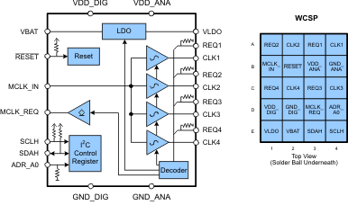
The CDC3S04 is a four-channel low-power low-jitter sine-wave clock buffer. It can be used
to buffer a single master clock to multiple peripherals. The four sine-wave outputs (CLK1–CLK4) are designed for minimal channel-to-channel skew and ultralow additive output jitter.Each output has its own clock request inputs which enables the dedicated clock output. These clock requests are active-high (can also be changed to be active-low via I2C), and an output signal is generated that can be sent back to the master clock to request the clock (MCLK_REQ). MCKL_REQ is an open-source output and supports the wired-OR function (default mode). It needs an external pulldown resistor. MCKL_REQ can be changed to wired-AND or push-pull functionality via I2C.The CDC3S04 also provides an I2C interface (Hs-mode) that can
be used to enable or disable the outputs, select the polarity of the REQ inputs, and allow control
of internal decoding.The CDC3S04 features an on-chip high-performance LDO that accepts voltages from 2.3 V to
5.5 V and outputs a 1.8-V supply. This 1.8-V supply can be used to power an external 1.8-V TCXO. It
can be enabled or disabled for power saving at the TCXO.A low signal at the RESET input switches the outputs CLK1 and CLK4 into the default state. In this configuration, CLK1 and CLK4 are ON (see ); the remaining device function is not affected. Also, the RESET input provides a glitch filter which rejects spikes of typical 300 ns on the RESET line to preserve false reset. A complete device reset to the default condition can be initiated by a power-up cycle of VDD_DIG.The CDC3S04 operates from two 1.8-V supplies. There is a core supply (VDD_DIG/GND_DIG)
for the core logic and a low-noise analog supply (VDD_ANA/GND_ANA) for the sine-wave outputs. The
CDC3S04 is designed for sequence-less power up. Both supply voltages may be applied in any order.The CDC3S04 is offered in a 0.4-mm pitch WCSP package (1.6 mm × 2 mm) and is optimized
for low standby current (0.5 µA). It is characterized for operation from –40°C to 85°C.
CDC3S04YFFR 电路图
CDC3S04YFFR 电路图
CDC3S04YFFR 相关产品
- ADCLK854BCPZ
- ADCLK907BCPZ-R2
- ADCLK907BCPZ-R7
- ADCLK914BCPZ-R2
- ADCLK914BCPZ-WP
- ADCLK925BCPZ-R7
- ADCLK944BCPZ-R2
- ADCLK944BCPZ-R7
- ADCLK944BCPZ-WP
- ADN4670BCPZ
- ADN4670BCPZ-REEL7
- CDC1104RVKR
- CDC111FN
- CDC204DW
- CDC204DWG4
- CDC208DW
- CDC208DWR
- CDC208NS
- CDC208NSR
- CDC2351DB
- CDC2351DBR
- CDC2351DW
- CDC2351DWR
- CDC2351DWRG4
- CDC2351MDBREP
- CDC2351QDB
- CDC2351QDBG4
- CDC2351QDBR
- CDC2351QDBRG4
- CDC318ADL