 搜索
搜索
 发布采购
发布采购
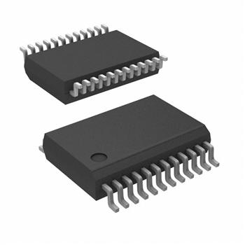
- 封装:24-SSOP(0.209",5.30mm 宽)
- RoHS:无铅 / 符合限制有害物质指令(RoHS)规范要求
- 包装方式:管件
- 参考价格:$10.108-$9.728
更新日期:2024-04-01 00:04:00
产品简介:具有三态输出的 1 线至 10 线 3.3V 时钟驱动器
查看详情- 封装:24-SSOP(0.209",5.30mm 宽)
- RoHS:无铅 / 符合限制有害物质指令(RoHS)规范要求
- 包装方式:管件
- 参考价格:$10.108-$9.728
CDC351IDB 供应商
- 公司
- 型号
- 品牌
- 封装/批号
- 数量
- 地区
- 日期
- 说明
- 询价
-
TI
-
原厂原装
22+ -
3288
-
上海市
-
-
-
一级代理原装
-
TI ?
-
SMD
5 -
50
-
杭州
-
-
-
原装正品现货
-
TI
-
-
2019+ -
5800
-
上海市
-
-
-
全新原装现货
-
TI(德州仪器)
-
SSOP-24
2022+ -
12000
-
上海市
-
-
-
原装可开发票
CDC351IDB 中文资料属性参数
- 标准包装:60
- 类别:集成电路 (IC)
- 家庭:时钟/计时 - 时钟缓冲器,驱动器
- 系列:-
- 类型:扇出缓冲器(分配)
- 电路数:1
- 比率 - 输入:输出:1:10
- 差分 - 输入:输出:无/无
- 输入:LVTTL
- 输出:LVTTL,三态
- 频率 - 最大:100MHz
- 电源电压:3 V ~ 3.6 V
- 工作温度:-40°C ~ 85°C
- 安装类型:表面贴装
- 封装/外壳:24-SSOP(0.209",5.30mm 宽)
- 供应商设备封装:24-SSOP
- 包装:管件
- 其它名称:296-15849-5
产品特性
- Low Output Skew, Low Pulse Skew for Clock-Distribution and Clock-Generation Applications
- Operates at 3.3-V VCC
- LVTTL-Compatible Inputs and Outputs
- Supports Mixed-Mode Signal Operation (5-V Input and Output Voltages With 3.3-V VCC)
- Distributes One Clock Input to Ten Outputs
- Distributed VCC and Ground Pins Reduce Switching Noise
- High-Drive Outputs (-32-mA IOH, 32-mA IOL)
- State-of-the-Art EPIC-IIBTM BiCMOS Design Significantly Reduces Power Dissipation
- Package Options Include Plastic Small-Outline (DW) and Shrink Small-Outline (DB) Packages
产品概述
The CDC351 is a high-performance clock-driver circuit that distributes one input (A) to ten outputs (Y) with minimum skew for clock distribution. The output-enable (OE)\ input disables the outputs to a high-impedance state. The CDC351 operates at nominal 3.3-V VCC.The propagation delays are adjusted at the factory using the P0 and P1 pins. The factory adjustments ensure that the part-to-part skew is minimized and is kept within a specified window. Pins P0 and P1 are not intended for customer use and should be connected to GND.
CDC351IDB 数据手册
 CDC351IDB
CDC351IDB 相关产品
- ADCLK854BCPZ
- ADCLK907BCPZ-R2
- ADCLK907BCPZ-R7
- ADCLK914BCPZ-R2
- ADCLK914BCPZ-WP
- ADCLK925BCPZ-R7
- ADCLK944BCPZ-R2
- ADCLK944BCPZ-R7
- ADCLK944BCPZ-WP
- ADN4670BCPZ
- ADN4670BCPZ-REEL7
- CDC1104RVKR
- CDC111FN
- CDC204DW
- CDC204DWG4
- CDC208DW
- CDC208DWR
- CDC208NS
- CDC208NSR
- CDC2351DB
- CDC2351DBR
- CDC2351DW
- CDC2351DWR
- CDC2351DWRG4
- CDC2351MDBREP
- CDC2351QDB
- CDC2351QDBG4
- CDC2351QDBR
- CDC2351QDBRG4
- CDC318ADL