 搜索
搜索
 发布采购
发布采购
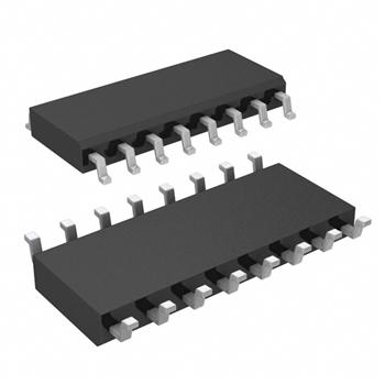
- 封装:16-SOIC(0.154",3.90mm 宽)
- RoHS:无铅 / 符合限制有害物质指令(RoHS)规范要求
- 包装方式:管件
- 参考价格:$3.7515-$7.63
更新日期:2024-04-01 00:04:00
产品简介:高速 CMOS 逻辑 4 x 4 寄存器文件
查看详情- 封装:16-SOIC(0.154",3.90mm 宽)
- RoHS:无铅 / 符合限制有害物质指令(RoHS)规范要求
- 包装方式:管件
- 参考价格:$3.7515-$7.63
CD74HCT670M 供应商
- 公司
- 型号
- 品牌
- 封装/批号
- 数量
- 地区
- 日期
- 说明
- 询价
-
TI
-
原厂原装
22+ -
3288
-
上海市
-
-
-
一级代理原装
-
TI
-
TSSOP
23+ -
46000
-
合肥
-
-
-
科大讯飞战略投资企业,提供一站式配套服务
CD74HCT670M 中文资料属性参数
- 标准包装:40
- 类别:集成电路 (IC)
- 家庭:逻辑 - 移位寄存器
- 系列:74HCT
- 逻辑类型:双向寄存器
- 输出类型:标准
- 元件数:1
- 每个元件的位元数:4
- 功能:通用
- 电源电压:4.5 V ~ 5.5 V
- 工作温度:-55°C ~ 125°C
- 安装类型:表面贴装
- 封装/外壳:16-SOIC(0.154",3.90mm 宽)
- 供应商设备封装:16-SOIC N
- 包装:管件
- 其它名称:296-9294-5
产品特性
- Simultaneous and Independent Read and Write Operations
- Expandable to 512 Words of n-Bits
- Three-State Outputs
- Organized as 4 Words x 4 Bits Wide
- Buffered Inputs
- Typical Read Time = 16ns for ’HC670 VCC = 5V, CL = 15pF, TA = 25°C
- Fanout (Over Temperature Range) Standard Outputs...10 LSTTL Loads Bus Driver Outputs...15 LSTTL Loads
- Standard Outputs...10 LSTTL Loads
- Bus Driver Outputs...15 LSTTL Loads
- Wide Operating Temperature Range... –55°C to 125°C
- Balanced Propagation Delay and Transition Times
- Significant Power Reduction Compared to LSTTL Logic ICs
- HC Types 2V to 6V Operation High Noise Immunity: NIL = 30%, NIH = 30% of VCC at VCC = 5V
- 2V to 6V Operation
- High Noise Immunity: NIL = 30%, NIH = 30% of VCC at VCC = 5V
- HCT Types 4.5V to 5.5V Operation Direct LSTTL Input Logic Compatibility, VIL = 0.8V (Max), VIH = 2V (Min) CMOS Input Compatibility, Il ≤ 1µA at VOL, VOH
- 4.5V to 5.5V Operation
- Direct LSTTL Input Logic Compatibility, VIL = 0.8V (Max), VIH = 2V (Min)
- CMOS Input Compatibility, Il ≤ 1µA at VOL, VOH
产品概述
The ’HC670 and CD74HCT670 are 16-bit register files organized as 4 words x 4 bits each. Read and write address and enable inputs allow simultaneous writing into one location while reading another. Four data inputs are provided to store the 4-bit word. The write address inputs (WA0 and WA1) determine the location of the stored word in the register. When write enable (WE\) is low the word is entered into the address location and it remains transparent to the data. The outputs will reflect the true form of the input data. When (WE\) is high data and address inputs are inhibited. Data acquisition from the four registers is made possible by the read address inputs (RA1 and RA0). The addressed word appears at the output when the read enable (RE\) is low. The output is in the high impedance state when the (RE\) is high. Outputs can be tied together to increase the word capacity to 512 x 4 bits.
CD74HCT670M 数据手册
| 数据手册 | 说明 | 数量 | 操作 |
|---|---|---|---|
 CD74HCT670M CD74HCT670M
|
High-Speed CMOS Logic 4x4 Register File |
14 Pages页,284K | 查看 |
|
CD74HCT670M
|
IC 4-BY-4 REGISTER FILE 16-SOIC |
16页,399K | 查看 |
|
CD74HCT670M96
|
High-Speed CMOS Logic 4x4 Register File |
14 Pages页,284K | 查看 |
|
CD74HCT670M96E4
|
High-Speed CMOS Logic 4x4 Register File |
14 Pages页,284K | 查看 |
|
CD74HCT670ME4
|
High-Speed CMOS Logic 4x4 Register File |
14 Pages页,284K | 查看 |
|
CD74HCT670MT
|
High-Speed CMOS Logic 4x4 Register File |
14 Pages页,284K | 查看 |
|
CD74HCT670MTE4
|
High-Speed CMOS Logic 4x4 Register File |
14 Pages页,284K | 查看 |
CD74HCT670M 相关产品
- 100336QC
- 74AC299SCX
- 74AHC164PW,118
- 74HC164PW,118
- 74HC165D,653
- 74HC4094PW,118
- 74HC595D,118
- 74HC595N,112
- 74HC597D,653
- 74HCT164D,653
- 74HCT165D,652
- 74HCT4015N,112
- 74HCT4094D,112
- 74HCT4094D,118
- 74HCT595N,112
- 74LV164D,118
- 74LV165PW,118
- 74LV595PW,112
- CD4014BE
- CD4014BM96
- CD4014BPWR
- CD4015BE
- CD4015BM96
- CD4015BM96G4
- CD4015BPWR
- CD40194BE
- CD4021BE
- CD4021BM96
- CD4021BM96E4
- CD4021BPWR