 搜索
搜索
 发布采购
发布采购
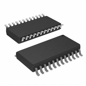
- 封装:24-SOIC(0.295",7.50mm 宽)
- RoHS:无铅 / 符合限制有害物质指令(RoHS)规范要求
- 包装方式:管件
- 参考价格:$2.97251
更新日期:2024-04-01 00:04:00
产品简介:具有三态输出的高速 CMOS 逻辑八通道总线收发器/寄存器
查看详情- 封装:24-SOIC(0.295",7.50mm 宽)
- RoHS:无铅 / 符合限制有害物质指令(RoHS)规范要求
- 包装方式:管件
- 参考价格:$2.97251
CD74HCT652M 供应商
- 公司
- 型号
- 品牌
- 封装/批号
- 数量
- 地区
- 日期
- 说明
- 询价
-
TI
-
原厂原装
22+ -
3288
-
上海市
-
-
-
一级代理原装
-
TI(德州仪器)
-
SOIC-24
2022+ -
12000
-
上海市
-
-
-
原装可开发票
CD74HCT652M 中文资料属性参数
- 标准包装:25
- 类别:集成电路 (IC)
- 家庭:逻辑 - 缓冲器,驱动器,接收器,收发器
- 系列:74HCT
- 逻辑类型:收发器,非反相
- 元件数:1
- 每个元件的位元数:8
- 输出电流高,低:6mA,6mA
- 电源电压:4.5 V ~ 5.5 V
- 工作温度:-55°C ~ 125°C
- 安装类型:表面贴装
- 封装/外壳:24-SOIC(0.295",7.50mm 宽)
- 供应商设备封装:24-SOIC
- 包装:管件
产品特性
- CD74HC652, CD74HCT652 . . . . . . . . . . . Non-Inverting
- Independent Registers for A and B Buses
- Three-State Outputs
- Drives 15 LSTTL Loads
- Typical Propagation Delay = 12ns at VCC =5V, CL = 15pF
- Fanout (Over Temperature Range) Standard Outputs . . . . . . . . . . . . . . . 10 LSTTL Loads Bus Driver Outputs . . . . . . . . . . . . . 15 LSTTL Loads
- Standard Outputs . . . . . . . . . . . . . . . 10 LSTTL Loads
- Bus Driver Outputs . . . . . . . . . . . . . 15 LSTTL Loads
- Wide Operating Temperature Range . . . -55°C to 125°C
- Balanced Propagation Delay and Transition Times
- Significant Power Reduction Compared to LSTTL Logic ICs
- Alternate Source is Philips
- HC Types 2V to 6V Operation High Noise Immunity: NIL = 30%, NIH = 30% of VCC at VCC = 5V
- 2V to 6V Operation
- High Noise Immunity: NIL = 30%, NIH = 30% of VCC at VCC = 5V
- HCT Types 4.5V to 5.5V Operation Direct LSTTL Input Logic Compatibility, VIL = 0.8V (Max), VIH = 2V (Min) CMOS Input Compatibility, Il ≤ 1µA at VOL, VOH
- 4.5V to 5.5V Operation
- Direct LSTTL Input Logic Compatibility, VIL = 0.8V (Max), VIH = 2V (Min)
- CMOS Input Compatibility, Il ≤ 1µA at VOL, VOH
产品概述
The CD74HC652 and CD74HCT652 three-state, octal-bus transceiver/registers use silicon-gate CMOS technology to achieve operating speeds similar to LSTTL with the low power consumption of standard CMOS integrated circuits. The CD74HC652 and CD74HCT652 have non-inverting outputs. These devices consists of bus transceiver circuits, D-type flip-flops, and control circuitry arranged for multiplexed transmission of data directly from the data bus or from the internal storage registers. Output Enables OEAB and OEBA are provided to control the transceiver functions. SAB and SBA control pins are provided to select whether real-time or stored data is transferred. The circuitry used for select control will eliminate the typical decoding glitch that occurs in a multiplexer during the transition between stored and real-time data. A LOW input level selects real-time data, and a HIGH selects stored data. The following examples demonstrates the four fundamentals bus-management functions that can be performed with the octal-bus transceivers and registers.Data on the A or B data bus, or both, can be stored in the internal D flip-flops by low-to-high transitions at the appropriate clock pins (CAB or CBA) regardless of the select of the control pins. When SAB and SBA are in the real-time transfer mode, it is also possible to store data without using the D-type flip-flops by simultaneously enabling OEAB and OEBA. In this configuration, each output reinforces its input. Thus, when all other data sources to the two sets of bus lines are at high impedance, each set of bus lines will remain at its last state.
CD74HCT652M 相关产品
- 100314QC
- 1P1G125QDCKRG4Q1
- 1P1G125QDCKRQ1
- 1P1G126QDBVRQ1
- 74ABT125PW,118
- 74ABT162244CSSX
- 74ABT162244DGGRG4
- 74ABT162245DLRG4
- 74ABT16245ADGGRG4
- 74ABT244D,623
- 74ABT245PW,118
- 74AC11244DBR
- 74AC11244DWR
- 74AC11244PWR
- 74AC11245DW
- 74AC11245DWR
- 74AC16244DGGR
- 74AC16244DL
- 74AC16244DLR
- 74AC16245DLR
- 74AC16652DL
- 74ACT11244DBR
- 74ACT11244DWR
- 74ACT11244PWR
- 74ACT11245DBR
- 74ACT11245DWR
- 74ACT11245NSR
- 74ACT11245PWR
- 74ACT16244DGGR
- 74ACT16244DLR