 搜索
搜索
 发布采购
发布采购
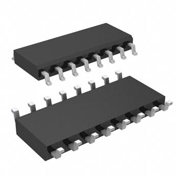
- 封装:16-SOIC(0.154",3.90mm 宽)
- RoHS:无铅 / 符合限制有害物质指令(RoHS)规范要求
- 包装方式:带卷 (TR)
- 参考价格:$0.334
更新日期:2024-04-01 00:04:00
产品简介:高速 CMOS 逻辑 4 位并行访问寄存器
查看详情- 封装:16-SOIC(0.154",3.90mm 宽)
- RoHS:无铅 / 符合限制有害物质指令(RoHS)规范要求
- 包装方式:带卷 (TR)
- 参考价格:$0.334
CD74HC195M96 供应商
- 公司
- 型号
- 品牌
- 封装/批号
- 数量
- 地区
- 日期
- 说明
- 询价
-
TI
-
原厂原装
22+ -
3288
-
上海市
-
-
-
一级代理原装
CD74HC195M96 中文资料属性参数
- 标准包装:2,500
- 类别:集成电路 (IC)
- 家庭:逻辑 - 移位寄存器
- 系列:74HC
- 逻辑类型:双向寄存器
- 输出类型:差分
- 元件数:1
- 每个元件的位元数:4
- 功能:通用
- 电源电压:2 V ~ 6 V
- 工作温度:-55°C ~ 125°C
- 安装类型:表面贴装
- 封装/外壳:16-SOIC(0.154",3.90mm 宽)
- 供应商设备封装:16-SOIC N
- 包装:带卷 (TR)
产品特性
- Asynchronous Master Reset
- J, K\,(D) Inputs to First Stage
- Fully Synchronous Serial or Parallel Data Transfer
- Shift Right and Parallel Load Capability
- Complementary Output From Last Stage
- Buffered Inputs
- Typical fMAX = 50MHz at VCC = 5V, CL = 15pF, TA = 25°C
- Fanout (Over Temperature Range) Standard Outputs . . . . 10 LSTTL Loads Bus Driver Outputs . . . . 15 LSTTL Loads
- Standard Outputs . . . . 10 LSTTL Loads
- Bus Driver Outputs . . . . 15 LSTTL Loads
- Wide Operating Temperature Range . . . –55°C to 125°C
- Balanced Propagation Delay and Transition Times
- Significant Power Reduction Compared to LSTTL Logic ICs
- HC Types 2V to 6V Operation High Noise Immunity: NIL = 30%, NIH = 30%of VCC at VCC = 5V
- 2V to 6V Operation
- High Noise Immunity: NIL = 30%, NIH = 30%of VCC at VCC = 5V
产品概述
The device is useful in a wide variety of shifting, counting and storage applications. It performs serial, parallel, serial to parallel, or parallel to serial data transfers at very high speeds.The two modes of operation, shift right (Q0-Q1) and parallel load, are controlled by the state of the Parallel Enable (PE)\ input. Serial data enters the first flip-flop (Q0) via the J and K\ inputs when the PE\ input is high, and is shifted one bit in the direction Q0-Q1-Q2-Q3 following each Low to High clock transition. The J and K\ inputs provide the flexibility of the JK-type input for special applications and by tying the two pins together, the simple D-type input for general applications. The device appears as four common-clocked D flip-flops when the PE\ input is Low. After the Low to High clock transition, data on the parallel inputs (D0-D3) is transferred to the respective Q0-Q3 outputs. Shift left operation (Q3-Q2) can be achieved by tying the Qn outputs to the Dn-1 inputs and holding the PE\ input low.All parallel and serial data transfers are synchronous, occurring after each Low to High clock transition. The ’HC195 series utilizes edge triggering; therefore, there is no restriction on the activity of the J, K\, Pn and PE\ inputs for logic operations, other than set-up and hold time requirements. A Low on the asynchronous Master Reset (MR)\ input sets all Q outputs Low, independent of any other input condition.
CD74HC195M96 数据手册
| 数据手册 | 说明 | 数量 | 操作 |
|---|---|---|---|
 CD74HC195M96 CD74HC195M96
|
IC 4-BIT ACCESS REGISTER 16SOIC |
16页,893K | 查看 |
CD74HC195M96 相关产品
- 100336QC
- 74AC299SCX
- 74AHC164PW,118
- 74HC164PW,118
- 74HC165D,653
- 74HC4094PW,118
- 74HC595D,118
- 74HC595N,112
- 74HC597D,653
- 74HCT164D,653
- 74HCT165D,652
- 74HCT4015N,112
- 74HCT4094D,112
- 74HCT4094D,118
- 74HCT595N,112
- 74LV164D,118
- 74LV165PW,118
- 74LV595PW,112
- CD4014BE
- CD4014BM96
- CD4014BPWR
- CD4015BE
- CD4015BM96
- CD4015BM96G4
- CD4015BPWR
- CD40194BE
- CD4021BE
- CD4021BM96
- CD4021BM96E4
- CD4021BPWR