 搜索
搜索
 发布采购
发布采购
- 封装:*
- RoHS:无铅 / 符合限制有害物质指令(RoHS)规范要求
- 包装方式:*
- 参考价格:$0.182-$0.51
更新日期:2024-04-01 00:04:00
产品简介:汽车类 20V、1:1 (SPST)、4 通道模拟开关
查看详情- 封装:*
- RoHS:无铅 / 符合限制有害物质指令(RoHS)规范要求
- 包装方式:*
- 参考价格:$0.182-$0.51
CD4066BQDRQ1 供应商
- 公司
- 型号
- 品牌
- 封装/批号
- 数量
- 地区
- 日期
- 说明
- 询价
-
TI
-
原厂原装
22+ -
3288
-
上海市
-
-
-
一级代理原装
-
TI
-
SMD
24+ -
2500
-
上海市
-
-
-
原装进口
CD4066BQDRQ1 中文资料属性参数
- 标准包装:1
- 类别:集成电路 (IC)
- 家庭:逻辑 - 信号开关,多路复用器,解码器
- 系列:4000B
- 类型:双向 FET 开关
- 电路:1 x 1:1
- 独立电路:4
- 输出电流高,低:-
- 电压电源:双电源
- 电源电压:3 V ~ 18 V
- 工作温度:-40°C ~ 125°C
- 安装类型:*
- 封装/外壳:*
- 供应商设备封装:*
- 包装:*
- 其它名称:296-31514-6
产品特性
- Qualified for Automotive Applications
- 15-V Digital or ±7.5-V Peak-to-Peak Switching
- 125-Ω Typical On-State Resistance for 15-V Operation
- Switch On-State Resistance Matched to Within 5 Ω Over 15-V Signal-Input Range
- On-State Resistance Flat Over Full Peak-to-Peak Signal Range
- High On/Off Output-Voltage Ratio: 80 dB Typical at fis = 10 kHz, RL = 1 kύ
- High Degree of Linearity: <0.5% Distortion Typical at fis = 1 kHz, Vis = 5 V p-p, VDD – VSS ≥ 10 V, RL = 10 kΩ
- Extremely Low Off-State Switch Leakage, Resulting in Very Low Offset Current and High Effective Off-State Resistance: 10 pA Typical at VDD – VSS = 10 V, TA = 25°C
- Extremely High Control Input Impedance (Control Circuit Isolated From Signal Circuit): 1012 Ω Typical
- Low Crosstalk Between Switches: –50 dB Typical at fis = 8 MHz, RL = 1 kΩ
- Matched Control-Input to Signal-Output Capacitance: Reduces Output Signal Transients
- Frequency Response, Switch On = 40 MHz Typical
- 100% Tested for Quiescent Current at 20 V
- 5-V, 10-V, and 15-V Parametric Ratings
- Latch-Up Exceeds 100mA per JESD78 - Class I
- Meets All Requirements of JEDEC Tentative Standard No. 13-B, Standard Specifications for Description of "B" Series CMOS Devices
- APPLICATIONS Analog Signal Switching/Multiplexing: Signal Gating, Modulator, Squelch Control, Demodulator, Chopper, Commutating Switch Digital Signal Switching/Multiplexing Transmission-Gate Logic Implementation Analog-to-Digital and Digital-to-Analog Conversion Digital Control of Frequency, Impedance, Phase, and Analog-Signal Gain
- Analog Signal Switching/Multiplexing: Signal Gating, Modulator, Squelch Control, Demodulator, Chopper, Commutating Switch
- Digital Signal Switching/Multiplexing
- Transmission-Gate Logic Implementation
- Analog-to-Digital and Digital-to-Analog Conversion
- Digital Control of Frequency, Impedance, Phase, and Analog-Signal Gain
产品概述
The CD4066B-Q1 is a quad bilateral switch intended for the transmission or multiplexing of analog or digital signals. It is pin-for-pin compatible with the CD4016B, but exhibits a much lower on-state resistance. In addition, the on-state resistance is relatively constant over the full signal-input range.The CD4066B-Q1 consists of four bilateral switches, each with independent controls. Both the p and the n devices in a given switch are biased on or off simultaneously by the control signal. As shown in , the well of the n-channel device on each switch is tied to either the input (when the switch is on) or to VSS (when the switch is off). This configuration eliminates the variation of the switch-transistor threshold voltage with input signal and, thus, keeps the on-state resistance low over the full operating-signal range.The advantages over single-channel switches include peak input-signal voltage swings equal to the full supply voltage and more constant on-state impedance over the input-signal range. However, for sample-and-hold applications, the CD4016B is recommended.
CD4066BQDRQ1 电路图
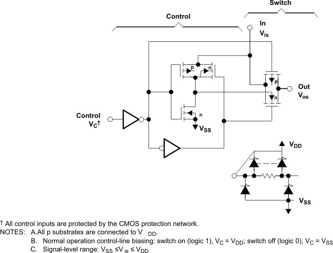
CD4066BQDRQ1 电路图
CD4066BQDRQ1 相关产品
- 74AC11138D
- 74AC11138DR
- 74AC11138N
- 74AC11138NSR
- 74AC11138PWR
- 74AC11257DW
- 74AC11257N
- 74AC11257PW
- 74AC139MTCX
- 74ACT11139D
- 74ACT11139PWR
- 74ACT11257DWR
- 74ACT138SJX
- 74ACT139MTCX
- 74ACT139SCX
- 74ACT257SCX
- 74AHC138D,118
- 74CB3Q16244DGGRG4
- 74CB3Q3125DBQRE4
- 74CB3Q3245RGYRG4
- 74CB3Q3257DBQRE4
- 74CB3Q3257RGYRG4
- 74CB3Q3305DCURG4
- 74CB3Q3306ADCURE4
- 74CB3Q3306ADCURG4
- 74CB3T16210DGGRG4
- 74CB3T16211DGGRE4
- 74CB3T1G125DBVRE4
- 74CB3T1G125DBVRG4
- 74CB3T1G125DCKRG4