 搜索
搜索
 发布采购
发布采购
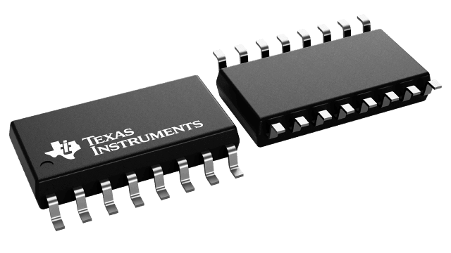
- 封装:16-SOIC(0.209",5.30mm 宽)
- RoHS:无铅 / 符合限制有害物质指令(RoHS)规范要求
- 包装方式:带卷 (TR)
- 参考价格:$0.18
更新日期:2024-04-01 00:04:00
产品简介:汽车类 CMOS 四路低向高电压位转换器(20V 额定电压)
查看详情- 封装:16-SOIC(0.209",5.30mm 宽)
- RoHS:无铅 / 符合限制有害物质指令(RoHS)规范要求
- 包装方式:带卷 (TR)
- 参考价格:$0.18
CD40109BQNSRQ1 供应商
- 公司
- 型号
- 品牌
- 封装/批号
- 数量
- 地区
- 日期
- 说明
- 询价
-
TI
-
原厂原装
22+ -
3288
-
上海市
-
-
-
一级代理原装
-
TI(德州仪器)
-
SO-16
2022+ -
12000
-
上海市
-
-
-
原装可开发票
CD40109BQNSRQ1 中文资料属性参数
- 标准包装:2,000
- 类别:集成电路 (IC)
- 家庭:逻辑 - 变换器
- 系列:4000B
- 逻辑功能:电平移位器,3 态
- 位数:4
- 输入类型:电压
- 输出类型:电压
- 数据速率:-
- 通道数:4
- 输出/通道数目:1
- 差分 - 输入:输出:无/无
- 传输延迟(最大):240ns
- 电源电压:3 V ~ 18 V
- 工作温度:-40°C ~ 125°C
- 封装/外壳:16-SOIC(0.209",5.30mm 宽)
- 供应商设备封装:16-SO
- 包装:带卷 (TR)
产品特性
- Qualified for Automotive Applications
- Independent of Power Supply Sequence Considerations VCC Can Exceed VDD Input Signals can Exceed Both VCC and VDD
- VCC Can Exceed VDD
- Input Signals can Exceed Both VCC and VDD
- Up and Down Level-Shifting Capability
- Three-State Outputs With Separate Enable Controls
- Standardized Symmetrical Output Characteristics
- 100% Tested for Quiescent Current at 20 V
- Maximum Input Current: 1 µA at 18 V Over Full Package-Temperature Range 100 nA at 18 V and 25°C
- 1 µA at 18 V Over Full Package-Temperature Range
- 100 nA at 18 V and 25°C
- Noise Margin (Full Package-Temperature Range): 1 V at VCC = 5 V, VDD = 10 V 2 V at VCC = 10 V, VDD = 15 V
- 1 V at VCC = 5 V, VDD = 10 V
- 2 V at VCC = 10 V, VDD = 15 V
- 5-V, 10-V, and 15-V Parametric Ratings
- Meets All Requirements of JEDEC Tentative Standard No. 13B, "Standard specifications for Description of ’B’ Series CMOS Devices"
- Latch-Up Performance Meets 50 mA per JESD 78, Class I
- APPLICATIONS High-or-Low Level-Shifting With Three-State Outputs for Unidirectional or Bidirectional Bussing Isolation of Logic Subsystem Using Separate Power Supplies from Supply Sequencing, Supply Loss, and Supply Regulation Considerations
- High-or-Low Level-Shifting With Three-State Outputs for Unidirectional or Bidirectional Bussing
- Isolation of Logic Subsystem Using Separate Power Supplies from Supply Sequencing, Supply Loss, and Supply Regulation Considerations
产品概述
CD40109B contains four low-to-high-voltage level-shifting circuits. Each circuit will shift a low-voltage digital-logic input signal (A, B, C, D) with logical 1 = VCC and logical 0 = VSS to a high-voltage output signal (E, F, G, H) with logical 1 = VDD and logical 0 = VSS.The RCA-CD40109, unlike other low-to-high level-shifting circuits, does not require the presence of the high-voltage supply (VDD) before the application of either the low-voltage supply (VCC) or the input signals. There are no restrictions on the sequence of application of VDD, VCC, or the input signals. In addition, with one exception there are no restrictions on the relative magnitudes of the supply voltages or input signals within the device maximum ratings, provided that the input signal swings between VSS and at least 0.7 VCC; VCC may exceed VDD, and input signals may exceed VCC and VDD. When operated in the mode VCC > VDD, the CD40109 will operate as a high-to-low level-shifter. The CD40109 also features individual three-state output capability. A low level on any of the separately enabled three-state output controls produces a high-impedance state in the corresponding output.
CD40109BQNSRQ1 相关产品
- 100324QC
- 100324SC
- 100325QC
- 100395QC
- 74ALVC164245DGG:11
- 74ALVC164245DGGRE4
- 74ALVC164245DGGRG4
- 74ALVC164245DGGTE4
- 74ALVC164245DGGTG4
- 74ALVC164245DL,118
- 74ALVC164245DLG4
- 74ALVC164245DLRG4
- 74AVC16T245DGVRE4
- 74AVC4T245BQ,115
- 74AVC4T245DGVRE4
- 74AVC4T245PW,118
- 74AVC4T245QRGYRQ1
- 74AVC4T245RGYRG4
- 74AVC4T245RSVRG4
- 74AVC4T774RSVRG4
- 74AVC8T245BQ,118
- 74AVC8T245RHLRG4
- 74AVCA164245GRE4
- 74AVCAH164245ZQLR
- 74AVCB164245GRE4
- 74AVCBH164245ZQLR
- 74AVCH1T45DBVRE4
- 74AVCH1T45DBVRG4
- 74AVCH1T45DCKRE4
- 74AVCH1T45DCKRG4