 搜索
搜索
 发布采购
发布采购
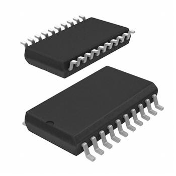
- 封装:20-SOIC(0.209",5.30mm 宽)
- RoHS:无铅 / 符合限制有害物质指令(RoHS)规范要求
- 包装方式:Digi-Reel®
- 参考价格:$1.656-$3.31
更新日期:2024-04-01 00:04:00
产品简介:具有清零功能的 3.3V Abt 八路 D 级触发器(增强型产品)
查看详情- 封装:20-SOIC(0.209",5.30mm 宽)
- RoHS:无铅 / 符合限制有害物质指令(RoHS)规范要求
- 包装方式:Digi-Reel®
- 参考价格:$1.656-$3.31
SN74LVTH273MNSREP 供应商
- 公司
- 型号
- 品牌
- 封装/批号
- 数量
- 地区
- 日期
- 说明
- 询价
-
TI
-
原厂原装
22+ -
3288
-
上海市
-
-
-
一级代理原装
SN74LVTH273MNSREP 中文资料属性参数
- 标准包装:1
- 类别:集成电路 (IC)
- 家庭:逻辑 - 触发器
- 系列:74LVTH
- 功能:主复位
- 类型:D 型总线
- 输出类型:非反相
- 元件数:1
- 每个元件的位元数:8
- 频率 - 时钟:150MHz
- 延迟时间 - 传输:3.2ns
- 触发器类型:正边沿
- 输出电流高,低:32mA,64mA
- 电源电压:2.7 V ~ 3.6 V
- 工作温度:-55°C ~ 125°C
- 安装类型:表面贴装
- 封装/外壳:20-SOIC(0.209",5.30mm 宽)
- 包装:®
- 其它名称:296-22393-6
产品特性
- Controlled Baseline One Assembly/Test Site, One Fabrication Site
- One Assembly/Test Site, One Fabrication Site
- Enhanced Diminishing Manufacturing Sources (DMS) Support
- Enhanced Product-Change Notification
- Qualification Pedigree
- Supports Mixed-Mode Signal Operation (5-V Input and Output Voltages With 3.3-V VCC)
- Typical VOLP (Output Ground Bounce) <0.8 V at VCC = 3.3 V, TA = 25°C
- Supports Unregulated Battery Operation Down to 2.7 V
- Buffered Clock and Direct-Clear Inputs
- Individual Data Input to Each Flip-Flop
- Ioff Supports Partial Power-Down-Mode Operation
- Bus Hold on Data Inputs Eliminates the Need for External Pullup/Pulldown Resistors
- Latch-Up Performance Exceeds 500 mA Per JESD 17
- ESD Protection Exceeds JESD 22 2000-V Human-Body Model (A114-A) 200-V Machine Model (A115-A)
- 2000-V Human-Body Model (A114-A)
- 200-V Machine Model (A115-A)
产品概述
This octal D-type flip-flop is designed specifically for low-voltage (3.3-V) VCC operation, but with the capability to provide a TTL interface to a 5-V system environment.The SN74LVTH273 is a positive-edge-triggered flip-flop with a direct-clear (CLR)\ input. Information at the data (D) inputs meeting the setup-time requirements is transferred to the Q outputs on the positive-going edge of the clock pulse. Clock triggering occurs at a particular voltage level and is not related directly to the transition time of the positive-going pulse. When the clock (CLK) input is at either the high or low level, the D-input signal has no effect at the output.Active bus-hold circuitry holds unused or undriven inputs at a valid logic state. Use of pullup or pulldown resistors with the bus-hold circuitry is not recommended.This device is fully specified for partial-power-down applications using Ioff. The Ioff circuitry disables the outputs, preventing damaging current backflow through the device when it is powered down.
SN74LVTH273MNSREP 数据手册
| 数据手册 | 说明 | 数量 | 操作 |
|---|---|---|---|
 SN74LVTH273MNSREP SN74LVTH273MNSREP
|
IC D-TYPE POS TRG SNGL 20SO |
10页,653K | 查看 |
SN74LVTH273MNSREP 相关产品
- 100331QC
- 100351QC
- 74ABT374CSCX
- 74AC11074D
- 74AC11074DR
- 74AC11074N
- 74AC11074PWR
- 74AC16374DLR
- 74AC273MTCX
- 74AC74MTR
- 74AC74SCX
- 74ACT11074D
- 74ACT11074DBR
- 74ACT11074N
- 74ACT11074NSR
- 74ACT11374DWR
- 74ACT16374DLR
- 74ACT16374DLRG4
- 74ACT16823DLR
- 74ACT574SJ
- 74ACT74MTCX
- 74ACT74TTR
- 74AHC1G79GV,125
- 74AHC377PW,118
- 74AHC574PW,118
- 74AHCT273PW,118
- 74AVC16722DGGRE4
- 74F175SCX
- 74F374SCX
- 74HC112PW,118