 搜索
搜索
 发布采购
发布采购
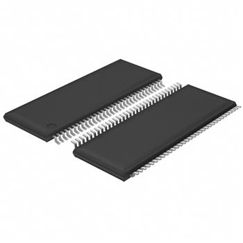
- 封装:64-TFSOP (0.240",6.10mm 宽)
- RoHS:无铅 / 符合限制有害物质指令(RoHS)规范要求
- 包装方式:带卷 (TR)
- 参考价格:$2.527
更新日期:2024-04-01 00:04:00
产品简介:具有三态输出的 22 位触发器
查看详情- 封装:64-TFSOP (0.240",6.10mm 宽)
- RoHS:无铅 / 符合限制有害物质指令(RoHS)规范要求
- 包装方式:带卷 (TR)
- 参考价格:$2.527
74AVC16722DGGRE4 供应商
- 公司
- 型号
- 品牌
- 封装/批号
- 数量
- 地区
- 日期
- 说明
- 询价
-
TI
-
原厂原装
22+ -
3288
-
上海市
-
-
-
一级代理原装
74AVC16722DGGRE4 中文资料属性参数
- 标准包装:2,000
- 类别:集成电路 (IC)
- 家庭:逻辑 - 触发器
- 系列:74AVC
- 功能:标准
- 类型:D 型总线
- 输出类型:三态非反相
- 元件数:1
- 每个元件的位元数:22
- 频率 - 时钟:80MHz
- 延迟时间 - 传输:7.7ns
- 触发器类型:正边沿
- 输出电流高,低:12mA,12mA
- 电源电压:1.4 V ~ 3.6 V
- 工作温度:-40°C ~ 85°C
- 安装类型:表面贴装
- 封装/外壳:64-TFSOP (0.240",6.10mm 宽)
- 包装:带卷 (TR)
产品特性
- Member of the Texas Instruments WidebusTM Family
- EPICTM (Enhanced-Performance Implanted CMOS) Submicron Process
- DOCTM (Dynamic Output Control) Circuit Dynamically Changes Output Impedance, Resulting in Noise Reduction Without Speed Degradation
- Dynamic Drive Capability Is Equivalent to Standard Outputs With IOH and IOL of ±24 mA at 2.5-V VCC
- Overvoltage-Tolerant Inputs/Outputs Allow Mixed-Voltage-Mode Data Communications
- Ioff Supports Partial-Power-Down Mode Operation
- Latch-Up Performance Exceeds 100 mA Per JESD 78, Class I
- Packaged in Thin Shrink Small-Outline Package DOC, EPIC, and Widebus are trademarks of Texas Instruments.
产品概述
A Dynamic Output Control (DOC) circuit is implemented, which, during the transition, initially lowers the output impedance to effectively drive the load and, subsequently, raises the impedance to reduce noise. Figure 1 shows typical VOL vs IOL and VOH vs IOH curves to illustrate the output impedance and drive capability of the circuit. At the beginning of the signal transition, the DOC circuit provides a maximum dynamic drive that is equivalent to a high-drive standard-output device. For more information, refer to the TI application reports,
AVC Logic Family Technology and Applications, literature number SCEA006, and
Dynamic Output Control (DOCTM
) Circuitry Technology and Applications, literature number SCEA009.
This 22-bit flip-flop is operational at 1.2-V to 3.6-V VCC, but is designed specifically for 1.65-V to 3.6-V VCC operation.
The 22 flip-flops of the SN74AVC16722 are edge-triggered D-type flip-flops with clock-enable (CLKEN\) input. On the positive transition of the clock (CLK) input, the device stores data into the flip-flops if CLKEN\ is low. If CLKEN\ is high, no data is stored.
A buffered output-enable (OE\) input places the 22 outputs in either a normal logic state (high or low) or the high-impedance state. In the high-impedance state, the outputs neither load nor drive the bus lines significantly. OE\ does not affect the internal operation of the flip-flops. Old data can be retained or new data can be entered while the outputs are in the high-impedance state.
To ensure the high-impedance state during power up or power down, OE\ should be tied to VCC through a pullup resistor; the minimum value of the resistor is determined by the current-sinking capability of the driver.
This device is fully specified for partial-power-down applications using Ioff. The Ioff circuitry disables the outputs, preventing damaging current backflow through the device when it is powered down.
The SN74AVC16722 is characterized for operation from -40°C to 85°C.
74AVC16722DGGRE4 数据手册
| 数据手册 | 说明 | 数量 | 操作 |
|---|---|---|---|
 74AVC16722DGGRE4 74AVC16722DGGRE4
|
22-BIT FLIP-FLOP WITH 3-STATE OUTPUTS |
1 Pages页,203K | 查看 |
74AVC16722DGGRE4 相关产品
- 100331QC
- 100351QC
- 74ABT374CSCX
- 74AC11074D
- 74AC11074DR
- 74AC11074N
- 74AC11074PWR
- 74AC16374DLR
- 74AC273MTCX
- 74AC74MTR
- 74AC74SCX
- 74ACT11074D
- 74ACT11074DBR
- 74ACT11074N
- 74ACT11074NSR
- 74ACT11374DWR
- 74ACT16374DLR
- 74ACT16374DLRG4
- 74ACT16823DLR
- 74ACT574SJ
- 74ACT74MTCX
- 74ACT74TTR
- 74AHC1G79GV,125
- 74AHC377PW,118
- 74AHC574PW,118
- 74AHCT273PW,118
- 74F175SCX
- 74F374SCX
- 74HC112PW,118
- 74HC173D,653