 搜索
搜索
 发布采购
发布采购
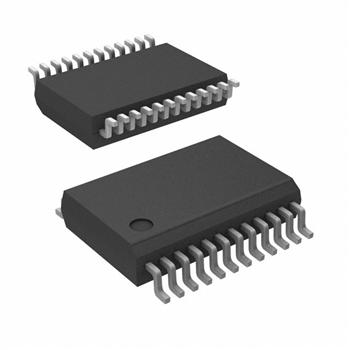
- 封装:24-SSOP(0.209",5.30mm 宽)
- RoHS:无铅 / 符合限制有害物质指令(RoHS)规范要求
- 包装方式:Digi-Reel®
- 参考价格:$0.4774-$1.11
更新日期:2024-04-01 00:04:00
产品简介:具有三态输出的 9 位总线接口触发器
查看详情- 封装:24-SSOP(0.209",5.30mm 宽)
- RoHS:无铅 / 符合限制有害物质指令(RoHS)规范要求
- 包装方式:Digi-Reel®
- 参考价格:$0.4774-$1.11
SN74LVC823ADBR 供应商
- 公司
- 型号
- 品牌
- 封装/批号
- 数量
- 地区
- 日期
- 说明
- 询价
-
TI
-
原厂原装
22+ -
3288
-
上海市
-
-
-
一级代理原装
SN74LVC823ADBR 中文资料属性参数
- 标准包装:1
- 类别:集成电路 (IC)
- 家庭:逻辑 - 触发器
- 系列:74LVC
- 功能:主复位
- 类型:D 型总线
- 输出类型:三态非反相
- 元件数:1
- 每个元件的位元数:9
- 频率 - 时钟:150MHz
- 延迟时间 - 传输:1.3ns
- 触发器类型:正边沿
- 输出电流高,低:24mA,24mA
- 电源电压:1.65 V ~ 3.6 V
- 工作温度:-40°C ~ 85°C
- 安装类型:表面贴装
- 封装/外壳:24-SSOP(0.209",5.30mm 宽)
- 包装:®
- 其它名称:296-8542-6
产品特性
- Operates From 1.65 V to 3.6 V
- Inputs Accept Voltages to 5.5 V
- Max tpd of 7.9 ns at 3.3 V
- Typical VOLP (Output Ground Bounce) <0.8 V at VCC = 3.3 V, TA = 25°C
- Typical VOHV (Output VOH Undershoot) >2 V at VCC = 3.3 V, TA = 25°C
- Supports Mixed-Mode Signal Operation on All Ports (5-V Input/Output Voltage With 3.3-V VCC)
- Ioff Supports Partial-Power-Down Mode Operation
- Latch-Up Performance Exceeds 250 mA Per JESD 17
- ESD Protection Exceeds JESD 22 2000-V Human-Body Model (A114-A) 200-V Machine Model (A115-A) 1000-V Charged-Device Model (C101)
- 2000-V Human-Body Model (A114-A)
- 200-V Machine Model (A115-A)
- 1000-V Charged-Device Model (C101)
产品概述
This 9-bit bus-interface flip-flop is designed for 1.65-V to 3.6-V VCC operation.The SN74LVC823A is designed specifically for driving highly capacitive or relatively low-impedance loads. It is particularly suitable for implementing wider buffer registers, I/O ports, bidirectional bus drivers with parity, and working registers.With the clock-enable (CLKEN)\ input low, the nine D-type edge-triggered flip-flops enter data on the low-to-high transitions of the clock. Taking CLKEN\ high disables the clock buffer, latching the outputs. This device has noninverting data (D) inputs. Taking the clear (CLR)\ input low causes the nine Q outputs to go low, independently of the clock.A buffered output-enable (OE)\ input can be used to place the nine outputs in either a normal logic state (high or low logic levels) or the high-impedance state. OE\ does not affect the internal operations of the latch. Previously stored data can be retained or new data can be entered while the outputs are in the high-impedance state.Inputs can be driven from either 3.3-V or 5-V devices. This feature allows the use of these devices as translators in a mixed 3.3-V/5-V system environment.This device is fully specified for partial-power-down applications using Ioff. The Ioff circuitry disables the outputs, preventing damaging current backflow through the device when it is powered down.To ensure the high-impedance state during power up or power down, OE\ should be tied to VCC through a pullup resistor; the minimum value of the resistor is determined by the current-sinking capability of the driver.
SN74LVC823ADBR 数据手册
| 数据手册 | 说明 | 数量 | 操作 |
|---|---|---|---|
 SN74LVC823ADBR SN74LVC823ADBR
|
9-BIT BUS-INTERFACE FLIP-FLOP WITH 3-STATE OUTPUTS |
14 Pages页,300K | 查看 |
|
SN74LVC823ADBR
|
IC D-TYPE POS TRG SNGL 24SSOP |
17页,626K | 查看 |
|
SN74LVC823ADBRE4
|
9-BIT BUS-INTERFACE FLIP-FLOP WITH 3-STATE OUTPUTS |
14 Pages页,300K | 查看 |
SN74LVC823ADBR 相关产品
- 100331QC
- 100351QC
- 74ABT374CSCX
- 74AC11074D
- 74AC11074DR
- 74AC11074N
- 74AC11074PWR
- 74AC16374DLR
- 74AC273MTCX
- 74AC74MTR
- 74AC74SCX
- 74ACT11074D
- 74ACT11074DBR
- 74ACT11074N
- 74ACT11074NSR
- 74ACT11374DWR
- 74ACT16374DLR
- 74ACT16374DLRG4
- 74ACT16823DLR
- 74ACT574SJ
- 74ACT74MTCX
- 74ACT74TTR
- 74AHC1G79GV,125
- 74AHC377PW,118
- 74AHC574PW,118
- 74AHCT273PW,118
- 74AVC16722DGGRE4
- 74F175SCX
- 74F374SCX
- 74HC112PW,118