 搜索
搜索
 发布采购
发布采购
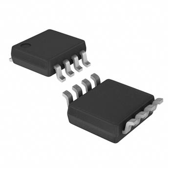
- 封装:8-VFSOP(0.091",2.30mm 宽)
- RoHS:无铅 / 符合限制有害物质指令(RoHS)规范要求
- 包装方式:Digi-Reel®
- 参考价格:$1.624-$2.23
更新日期:2024-04-01 00:04:00
产品简介:具有清零和预置端的单路正边沿触发式 D 型触发器(增强型产品)
查看详情- 封装:8-VFSOP(0.091",2.30mm 宽)
- RoHS:无铅 / 符合限制有害物质指令(RoHS)规范要求
- 包装方式:Digi-Reel®
- 参考价格:$1.624-$2.23
SN74LVC2G74MDCUTEP 供应商
- 公司
- 型号
- 品牌
- 封装/批号
- 数量
- 地区
- 日期
- 说明
- 询价
-
TI
-
原厂原装
22+ -
3288
-
上海市
-
-
-
一级代理原装
-
TI(德州仪器)
-
VSSOP-8
2022+ -
12000
-
上海市
-
-
-
原装可开发票
SN74LVC2G74MDCUTEP 中文资料属性参数
- 标准包装:1
- 类别:集成电路 (IC)
- 家庭:逻辑 - 触发器
- 系列:74LVC
- 功能:设置(预设)和复位
- 类型:D 型
- 输出类型:差分
- 元件数:1
- 每个元件的位元数:1
- 频率 - 时钟:200MHz
- 延迟时间 - 传输:4.1ns
- 触发器类型:正边沿
- 输出电流高,低:32mA,32mA
- 电源电压:1.65 V ~ 5.5 V
- 工作温度:-55°C ~ 125°C
- 安装类型:表面贴装
- 封装/外壳:8-VFSOP(0.091",2.30mm 宽)
- 包装:®
- 其它名称:296-23740-6
产品特性
- Controlled Baseline One Assembly Site One Test Site One Fabrication Site
- One Assembly Site
- One Test Site
- One Fabrication Site
- Extended Temperature Performance of –55°C to 125°C
- Enhanced Diminishing Manufacturing Sources (DMS) Support
- Enhanced Product-Change Notification
- Qualification Pedigree(1)
- Supports 5-V VCC Operation
- Inputs Accept Voltages to 5.5 V
- Max tpd of 7.9 ns at 3.3 V
- Low Power Consumption, 10 µA Max ICC
- ±24 mA Output Drive at 3.3 V
- Typical VOLP (Output Ground Bounce) <0.8 V at VCC = 3.3 V, TA = 25°C
- Typical VOHV (Output VOH Undershoot) >2 V at VCC = 3.3 V, TA = 25°C
- Ioff Supports Partial Power Down Mode Operation
- Latch-Up Performance Exceeds 100 mA Per JESD 78, Class II
- ESD Protection Exceeds JESD 22 2000-V Human-Body Model (A114-A) 200-V Machine Model (A115-A) 1000-V Charged-Device Model (C101)
- 2000-V Human-Body Model (A114-A)
- 200-V Machine Model (A115-A)
- 1000-V Charged-Device Model (C101)
产品概述
This single positive edge triggered D-type flip-flop is designed for 1.65-V to 5.5-V VCC operation.A low level at the preset (PRE) or clear (CLR) input sets or resets the outputs, regardless of the levels of the other inputs. When PRE and CLR are inactive (high), data at the data (D) input meeting the setup time requirements is transferred to the outputs on the positive-going edge of the clock pulse. Clock triggering occurs at a voltage level and is not related directly to the rise time of the clock pulse. Following the hold-time interval, data at the D input can be changed without affecting the levels at the outputs.This device is fully specified for partial power down applications using Ioff. The Ioff circuitry disables the outputs, preventing damaging current backflow through the device when it is powered down.
SN74LVC2G74MDCUTEP 数据手册
| 数据手册 | 说明 | 数量 | 操作 |
|---|---|---|---|
 SN74LVC2G74MDCUTEP SN74LVC2G74MDCUTEP
|
IC D-TYPE POS TRG SNGL US8 |
12页,748K | 查看 |
SN74LVC2G74MDCUTEP 相关产品
- 100331QC
- 100351QC
- 74ABT374CSCX
- 74AC11074D
- 74AC11074DR
- 74AC11074N
- 74AC11074PWR
- 74AC16374DLR
- 74AC273MTCX
- 74AC74MTR
- 74AC74SCX
- 74ACT11074D
- 74ACT11074DBR
- 74ACT11074N
- 74ACT11074NSR
- 74ACT11374DWR
- 74ACT16374DLR
- 74ACT16374DLRG4
- 74ACT16823DLR
- 74ACT574SJ
- 74ACT74MTCX
- 74ACT74TTR
- 74AHC1G79GV,125
- 74AHC377PW,118
- 74AHC574PW,118
- 74AHCT273PW,118
- 74AVC16722DGGRE4
- 74F175SCX
- 74F374SCX
- 74HC112PW,118