 搜索
搜索
 发布采购
发布采购
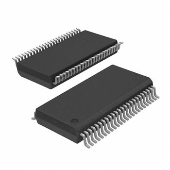
- 封装:48-TFSOP(0.240",6.10mm 宽)
- RoHS:无铅 / 符合限制有害物质指令(RoHS)规范要求
- 包装方式:Digi-Reel®
- 参考价格:$0.589-$1.37
更新日期:2024-04-01 00:04:00
产品简介:具有三态输出的 16 位边沿 D 类触发器
查看详情- 封装:48-TFSOP(0.240",6.10mm 宽)
- RoHS:无铅 / 符合限制有害物质指令(RoHS)规范要求
- 包装方式:Digi-Reel®
- 参考价格:$0.589-$1.37
SN74LVC16374DGGR 供应商
- 公司
- 型号
- 品牌
- 封装/批号
- 数量
- 地区
- 日期
- 说明
- 询价
-
TI
-
原厂原装
22+ -
3288
-
上海市
-
-
-
一级代理原装
-
TI(德州仪器)
-
TSSOP-48
2022+ -
693
-
上海市
-
-
-
原装可开发票
-
TI
-
-
2021+ -
28000
-
苏州
-
-
SN74LVC16374DGGR 中文资料属性参数
- 标准包装:1
- 类别:集成电路 (IC)
- 家庭:逻辑 - 触发器
- 系列:74LVC
- 功能:标准
- 类型:D 型总线
- 输出类型:三态非反相
- 元件数:2
- 每个元件的位元数:8
- 频率 - 时钟:150MHz
- 延迟时间 - 传输:1.5ns
- 触发器类型:正边沿
- 输出电流高,低:24mA,24mA
- 电源电压:1.65 V ~ 3.6 V
- 工作温度:-40°C ~ 85°C
- 安装类型:表面贴装
- 封装/外壳:48-TFSOP(0.240",6.10mm 宽)
- 包装:®
- 其它名称:296-11833-6
产品特性
- Member of the Texas Instruments WidebusTM Family
- EPICTM (Enhanced-Performance Implanted CMOS) Submicron Process
- Typical VOLP (Output Ground Bounce) < 0.8 V at VCC = 3.3 V, TA = 25°C
- Typical VOHV (Output VOH Undershoot) > 2 V at VCC = 3.3 V, TA = 25°C
- Latch-Up Performance Exceeds 250 mA Per JEDEC Standard JESD-17
- Bus Hold on Data Inputs Eliminates the Need for External Pullup/Pulldown Resistors
- Package Options Include Plastic 300-mil Shrink Small-Outline (DL) and Thin Shrink Small-Outline (DGG) Packages EPIC and Widebus are trademarks of Texas Instruments Incorporated.
产品概述
This 16-bit edge-triggered D-type flip-flop is designed for 2.7-V to 3.6-V VCC operation.
The SN74LVC16374 is particularly suitable for implementing buffer registers, I/O ports, bidirectional bus drivers, and working registers. It can be used as two 8-bit flip-flops or one 16-bit flip-flop. On the positive transition of the clock (CLK) input, the Q outputs of the flip-flop take on the logic levels set up at the data (D) inputs.
A buffered output-enable (OE\) input can be used to place the eight outputs in either a normal logic state (high or low logic levels) or a high-impedance state. In the high-impedance state, the outputs neither load nor drive the bus lines significantly. The high-impedance state and the increased drive provide the capability to drive bus lines without need for interface or pullup components.
OE\ does not affect internal operations of the flip-flop. Old data can be retained or new data can be entered while the outputs are in the high-impedance state.
To ensure the high-impedance state during power up or power down, OE\ should be tied to VCC through a pullup resistor; the minimum value of the resistor is determined by the current-sinking capability of the driver.
Active bus-hold circuitry is provided to hold unused or floating data inputs at a valid logic level.
The SN74LVC16374 is characterized for operation from -40°C to 85°C.
SN74LVC16374DGGR 相关产品
- 100331QC
- 100351QC
- 74ABT374CSCX
- 74AC11074D
- 74AC11074DR
- 74AC11074N
- 74AC11074PWR
- 74AC16374DLR
- 74AC273MTCX
- 74AC74MTR
- 74AC74SCX
- 74ACT11074D
- 74ACT11074DBR
- 74ACT11074N
- 74ACT11074NSR
- 74ACT11374DWR
- 74ACT16374DLR
- 74ACT16374DLRG4
- 74ACT16823DLR
- 74ACT574SJ
- 74ACT74MTCX
- 74ACT74TTR
- 74AHC1G79GV,125
- 74AHC377PW,118
- 74AHC574PW,118
- 74AHCT273PW,118
- 74AVC16722DGGRE4
- 74F175SCX
- 74F374SCX
- 74HC112PW,118