 搜索
搜索
 发布采购
发布采购
- 封装:*
- RoHS:无铅 / 符合限制有害物质指令(RoHS)规范要求
- 包装方式:*
- 参考价格:$0.5782-$0.86
更新日期:2024-04-01 00:04:00
产品简介:低功耗单路上升沿 D 级触发器
查看详情- 封装:*
- RoHS:无铅 / 符合限制有害物质指令(RoHS)规范要求
- 包装方式:*
- 参考价格:$0.5782-$0.86
SN74AUP1G79DBVT 供应商
- 公司
- 型号
- 品牌
- 封装/批号
- 数量
- 地区
- 日期
- 说明
- 询价
-
TI
-
原厂原装
22+ -
3288
-
上海市
-
-
-
一级代理原装
SN74AUP1G79DBVT 中文资料属性参数
- 标准包装:1
- 类别:集成电路 (IC)
- 家庭:逻辑 - 触发器
- 系列:74AUP
- 功能:标准
- 类型:D 型
- 输出类型:非反相
- 元件数:1
- 每个元件的位元数:1
- 频率 - 时钟:280MHz
- 延迟时间 - 传输:3ns
- 触发器类型:正边沿
- 输出电流高,低:4mA,4mA
- 电源电压:0.8 V ~ 3.6 V
- 工作温度:-40°C ~ 85°C
- 安装类型:*
- 封装/外壳:*
- 包装:*
- 其它名称:296-32263-6
产品特性
- Available in the Texas Instruments NanoStar™ Package
- Low Static-Power Consumption: ICC = 0.9 µA Maximum
- Low Dynamic-Power Consumption: Cpd = 3 pF Typical at 3.3 V
- Low Input Capacitance: Ci = 1.5 pF Typical
- Low Noise: Overshoot and Undershoot < 10% of VCC
- Ioff Supports Partial Power-Down-Mode Operation
- Input Hysteresis Allows Slow Input Transition and Better Switching Noise Immunity at the Input (Vhys = 250 mV Typical at 3.3 V)
- Wide Operating VCC Range of 0.8 V to 3.6 V
- Optimized for 3.3-V Operation
- 3.6-V I/O Tolerant to Support Mixed-Mode Signal Operation
- tpd = 4 ns Maximum at 3.3 V
- Suitable for Point-to-Point Applications
- Latch-Up Performance Exceeds 100 mA Per JESD 78, Class II
- ESD Performance Tested Per JESD 22 2000-V Human-Body Model (A114-B, Class II) 1000-V Charged-Device Model (C101)
- 2000-V Human-Body Model (A114-B, Class II)
- 1000-V Charged-Device Model (C101)
产品概述
The AUP family is TI’s premier solution to the industry’s low-power needs in
battery-powered portable applications. This family assures a very-low static and dynamic power
consumption across the entire VCC range of 0.8 V to 3.6 V, thus resulting in
an increased battery life. The AUP devices also maintain excellent signal integrity.The SN74AUP1G79 is a single positive-edge-triggered D-type flip-flop. When data at the
data (D) input meets the setup-time requirement, the data is transferred to the Q output on the
positive-going edge of the clock pulse. Clock triggering occurs at a voltage level and is not
directly related to the rise time of the clock pulse. Following the hold-time interval, data at the
D input can be changed without affecting the levels at the outputs.NanoStar™ package technology is a major breakthrough in IC packaging concepts, using the
die as the package.The SN74AUP1G79 device is fully specified for partial-power-down applications using
Ioff. The Ioff circuitry disables the outputs when
the device is powered down. This inhibits current backflow into the device which prevents damage to
the device.
SN74AUP1G79DBVT 数据手册
| 数据手册 | 说明 | 数量 | 操作 |
|---|---|---|---|
 SN74AUP1G79DBVT SN74AUP1G79DBVT
|
LOW POWER SINGLE POSITIVE EDGE TRIGGERRED D TYPE FLIP FLOP |
15 Pages页,267K | 查看 |
|
SN74AUP1G79DBVT
|
IC D-TYPE POS TRG SNGL SOT23-5 |
36页,1.43M | 查看 |
|
SN74AUP1G79DBVTE4
|
LOW POWER SINGLE POSITIVE EDGE TRIGGERRED D TYPE FLIP FLOP |
15 Pages页,267K | 查看 |
SN74AUP1G79DBVT 电路图
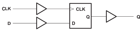
SN74AUP1G79DBVT 电路图
SN74AUP1G79DBVT 相关产品
- 100331QC
- 100351QC
- 74ABT374CSCX
- 74AC11074D
- 74AC11074DR
- 74AC11074N
- 74AC11074PWR
- 74AC16374DLR
- 74AC273MTCX
- 74AC74MTR
- 74AC74SCX
- 74ACT11074D
- 74ACT11074DBR
- 74ACT11074N
- 74ACT11074NSR
- 74ACT11374DWR
- 74ACT16374DLR
- 74ACT16374DLRG4
- 74ACT16823DLR
- 74ACT574SJ
- 74ACT74MTCX
- 74ACT74TTR
- 74AHC1G79GV,125
- 74AHC377PW,118
- 74AHC574PW,118
- 74AHCT273PW,118
- 74AVC16722DGGRE4
- 74F175SCX
- 74F374SCX
- 74HC112PW,118