 搜索
搜索
 发布采购
发布采购
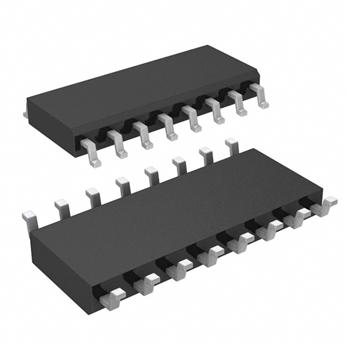
- 封装:16-SOIC(0.154",3.90mm 宽)
- RoHS:无铅 / 符合限制有害物质指令(RoHS)规范要求
- 包装方式:管件
- 参考价格:$2.1525
更新日期:2024-04-01 00:04:00
产品简介:具有清零和预设功能的双通道 J-K 上升沿触发器
查看详情- 封装:16-SOIC(0.154",3.90mm 宽)
- RoHS:无铅 / 符合限制有害物质指令(RoHS)规范要求
- 包装方式:管件
- 参考价格:$2.1525
SN74AS109AD 供应商
- 公司
- 型号
- 品牌
- 封装/批号
- 数量
- 地区
- 日期
- 说明
- 询价
-
TI
-
原厂原装
22+ -
3288
-
上海市
-
-
-
一级代理原装
SN74AS109AD 中文资料属性参数
- 标准包装:40
- 类别:集成电路 (IC)
- 家庭:逻辑 - 触发器
- 系列:74AS
- 功能:设置(预设)和复位
- 类型:JK 型
- 输出类型:差分
- 元件数:2
- 每个元件的位元数:1
- 频率 - 时钟:105MHz
- 延迟时间 - 传输:2.5ns
- 触发器类型:正边沿
- 输出电流高,低:2mA,20mA
- 电源电压:4.5 V ~ 5.5 V
- 工作温度:0°C ~ 70°C
- 安装类型:表面贴装
- 封装/外壳:16-SOIC(0.154",3.90mm 宽)
- 包装:管件
- 其它名称:296-6331-5
产品特性
- Package Options Include Plastic Small-Outline (D) Packages, Ceramic Chip Carriers (FK), and Standard Plastic (N) and Ceramic (J) 300-mil DIPs
产品概述
SN74AS109AD 数据手册
| 数据手册 | 说明 | 数量 | 操作 |
|---|---|---|---|
 SN74AS109AD SN74AS109AD
|
DUAL J-K POSITIVE-EDGE-TRIGGERED FLIP-FLOPS WITH CLEAR AND PRESET |
9 Pages页,139K | 查看 |
|
SN74AS109ADE4
|
Dual J-K Positive-Edge-Triggered Flip-Flops With Clear And Preset 16-SOIC 0 to 70 |
17页,684K | 查看 |
|
SN74AS109ADG4
|
Dual J-K Positive-Edge-Triggered Flip-Flops With Clear And Preset 16-SOIC 0 to 70 |
17页,684K | 查看 |
|
SN74AS109ADR
|
DUAL J-K POSITIVE-EDGE-TRIGGERED FLIP-FLOPS WITH CLEAR AND PRESET |
9 Pages页,139K | 查看 |
|
SN74AS109ADRE4
|
These devices contain two independent J-K\ positive-edge-triggered flip-flops. A low level at the preset () or clear () inputs sets or resets the outputs regardless of the levels of the other inputs. When and are inactive (high), data at the J and K\ inputs meeting the setup-time requirements are transferred to the outputs on the positive-going edge of the clock (CLK) pulse. Clock triggering occurs at a voltage level and is not directly related to the rise time of the clock pulse. Following the hold-time interval, data at the J and K\ inputs can be changed without affecting the levels at the... |
17页,684K | 查看 |
|
SN74AS109ADRG4
|
These devices contain two independent J-K\ positive-edge-triggered flip-flops. A low level at the preset () or clear () inputs sets or resets the outputs regardless of the levels of the other inputs. When and are inactive (high), data at the J and K\ inputs meeting the setup-time requirements are transferred to the outputs on the positive-going edge of the clock (CLK) pulse. Clock triggering occurs at a voltage level and is not directly related to the rise time of the clock pulse. Following the hold-time interval, data at the J and K\ inputs can be changed without affecting the levels at the... |
17页,684K | 查看 |
SN74AS109AD 相关产品
- 100331QC
- 100351QC
- 74ABT374CSCX
- 74AC11074D
- 74AC11074DR
- 74AC11074N
- 74AC11074PWR
- 74AC16374DLR
- 74AC273MTCX
- 74AC74MTR
- 74AC74SCX
- 74ACT11074D
- 74ACT11074DBR
- 74ACT11074N
- 74ACT11074NSR
- 74ACT11374DWR
- 74ACT16374DLR
- 74ACT16374DLRG4
- 74ACT16823DLR
- 74ACT574SJ
- 74ACT74MTCX
- 74ACT74TTR
- 74AHC1G79GV,125
- 74AHC377PW,118
- 74AHC574PW,118
- 74AHCT273PW,118
- 74AVC16722DGGRE4
- 74F175SCX
- 74F374SCX
- 74HC112PW,118