 搜索
搜索
 发布采购
发布采购
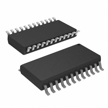
- 封装:24-SOIC(0.295",7.50mm 宽)
- RoHS:无铅 / 符合限制有害物质指令(RoHS)规范要求
- 包装方式:Digi-Reel®
- 参考价格:$0.9685-$2.07
更新日期:2024-04-01 00:04:00
产品简介:具有三态输出的 9 位总线接口触发器
查看详情- 封装:24-SOIC(0.295",7.50mm 宽)
- RoHS:无铅 / 符合限制有害物质指令(RoHS)规范要求
- 包装方式:Digi-Reel®
- 参考价格:$0.9685-$2.07
SN74ABT823DWR 供应商
- 公司
- 型号
- 品牌
- 封装/批号
- 数量
- 地区
- 日期
- 说明
- 询价
-
TI
-
原厂原装
22+ -
3288
-
上海市
-
-
-
一级代理原装
-
TI(德州仪器)
-
SOIC-24
2022+ -
12000
-
上海市
-
-
-
原装可开发票
SN74ABT823DWR 中文资料属性参数
- 标准包装:1
- 类别:集成电路 (IC)
- 家庭:逻辑 - 触发器
- 系列:74ABT
- 功能:主复位
- 类型:D 型总线
- 输出类型:三态非反相
- 元件数:1
- 每个元件的位元数:9
- 频率 - 时钟:200MHz
- 延迟时间 - 传输:4.3ns
- 触发器类型:正边沿
- 输出电流高,低:32mA,64mA
- 电源电压:4.5 V ~ 5.5 V
- 工作温度:-40°C ~ 85°C
- 安装类型:表面贴装
- 封装/外壳:24-SOIC(0.295",7.50mm 宽)
- 包装:®
- 其它名称:296-14678-6
产品特性
- State-of-the-Art EPIC-II BTM BiCMOS Design Significantly Reduces Power Dissipation
- ESD Protection Exceeds 2000 V Per MIL-STD-883, Method 3015; Exceeds 200 V Using Machine Model (C = 200 pF, R = 0)
- Latch-Up Performance Exceeds 500 mA Per JEDEC Standard JESD-17
- Typical VOLP (Output Ground Bounce) < 1 V at VCC = 5 V, TA = 25°C
- High-Impedance State During Power Up and Power Down
- High-Drive Outputs (-32-mA IOH, 64-mA IOL)
- Buffered Control Inputs to Reduce dc Loading Effects
- Package Options Include Plastic Small-Outline (DW) and Shrink Small-Outline (DB) Packages, Ceramic Chip Carriers (FK) and Flatpacks (W), and Standard Plastic (NT) and Ceramic (JT) DIPs
产品概述
These 9-bit flip-flops feature 3-state outputs designed specifically for driving highly capacitive or relatively low-impedance loads. They are particularly suitable for implementing wider buffer registers, I/O ports, bidirectional bus drivers with parity, and working registers.
With the clock-enable (CLKEN\) input low, the nine D-type edge-triggered flip-flops enter data on the low-to-high transitions of the clock. Taking CLKEN\ high disables the clock buffer, thus latching the outputs. Taking the clear (CLR\) input low causes the nine Q outputs to go low, independently of the clock.
A buffered output-enable (OE\) input can be used to place the nine outputs in either a normal logic state (high or low logic level) or a high-impedance state. In the high-impedance state, the outputs neither load nor drive the bus lines significantly. The high-impedance state and increased drive provide the capability to drive bus lines without need for interface or pullup components.
When VCC is between 0 and 2.1 V, the device is in the high-impedance state during power up or power down. However, to ensure the high-impedance state above 2.1 V, OE\ should be tied to VCC through a pullup resistor; the minimum value of the resistor is determined by the current-sinking capability of the driver.
The SN54ABT823 is characterized for operation over the full military temperature range of -55°C to 125°C. The SN74ABT823 is characterized for operation from -40°C to 85°C.
SN74ABT823DWR 数据手册
| 数据手册 | 说明 | 数量 | 操作 |
|---|---|---|---|
 SN74ABT823DWR SN74ABT823DWR
|
9-Bit Bus-Interface Flip-Flops With 3-State Outputs 24-SOIC -40 to 85 |
18页,571K | 查看 |
|
SN74ABT823DWR
|
IC D-TYPE POS TRG SNGL 24SOIC |
18页,660K | 查看 |
|
SN74ABT823DWRE4
|
9-Bit Bus-Interface Flip-Flops With 3-State Outputs 24-SOIC -40 to 85 |
18页,571K | 查看 |
SN74ABT823DWR 相关产品
- 100331QC
- 100351QC
- 74ABT374CSCX
- 74AC11074D
- 74AC11074DR
- 74AC11074N
- 74AC11074PWR
- 74AC16374DLR
- 74AC273MTCX
- 74AC74MTR
- 74AC74SCX
- 74ACT11074D
- 74ACT11074DBR
- 74ACT11074N
- 74ACT11074NSR
- 74ACT11374DWR
- 74ACT16374DLR
- 74ACT16374DLRG4
- 74ACT16823DLR
- 74ACT574SJ
- 74ACT74MTCX
- 74ACT74TTR
- 74AHC1G79GV,125
- 74AHC377PW,118
- 74AHC574PW,118
- 74AHCT273PW,118
- 74AVC16722DGGRE4
- 74F175SCX
- 74F374SCX
- 74HC112PW,118